Northrop Grumman opens access to US chip facilities
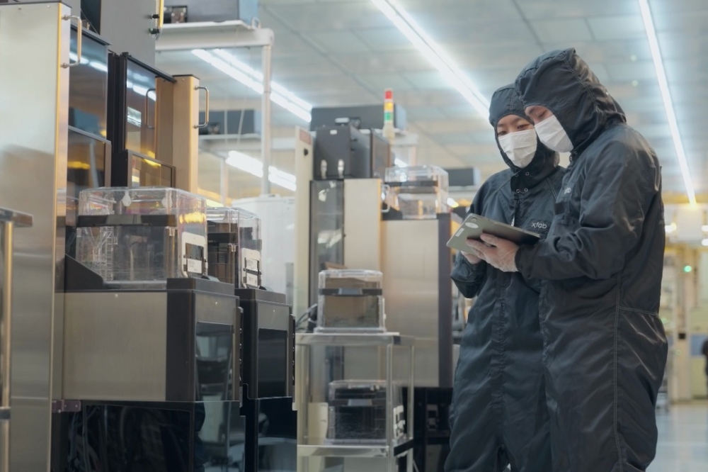
Northrop Grumman has announced that its Microelectronics Centre is now open for external aerospace and defence companies to access the company’s three US government-accredited semiconductor manufacturing facilities.
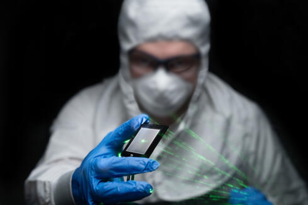
According to the company, this decision expands the secure production of defence microelectronics on US soil.
The open-access business model allows commercial businesses, aerospace and defence companies, the US Government, academia, federally funded research and development centres and others, to design, manufacture, package and test microelectronics domestically for commercial and defence applications.
It will also give access to end-to-end US-based advanced packaging facilities with reliable semiconductor design, post-processing, assembly and test for current and future generation technologies.
Northrop Grumman-produced semiconductor products and components will also be available for purchase via an online storefront.
Vern Boyle, vice president of the Northrop Grumman Microelectronics centre: “By opening our defence-grade manufacturing facilities to partners, Northrop Grumman is expanding and strengthening the resilience of America's semiconductor industry and supply chain. We are providing partners with unprecedented access to design and develop domestic chips as well as the ability to directly purchase from us, enhancing collaboration across the broader defence industrial base.”
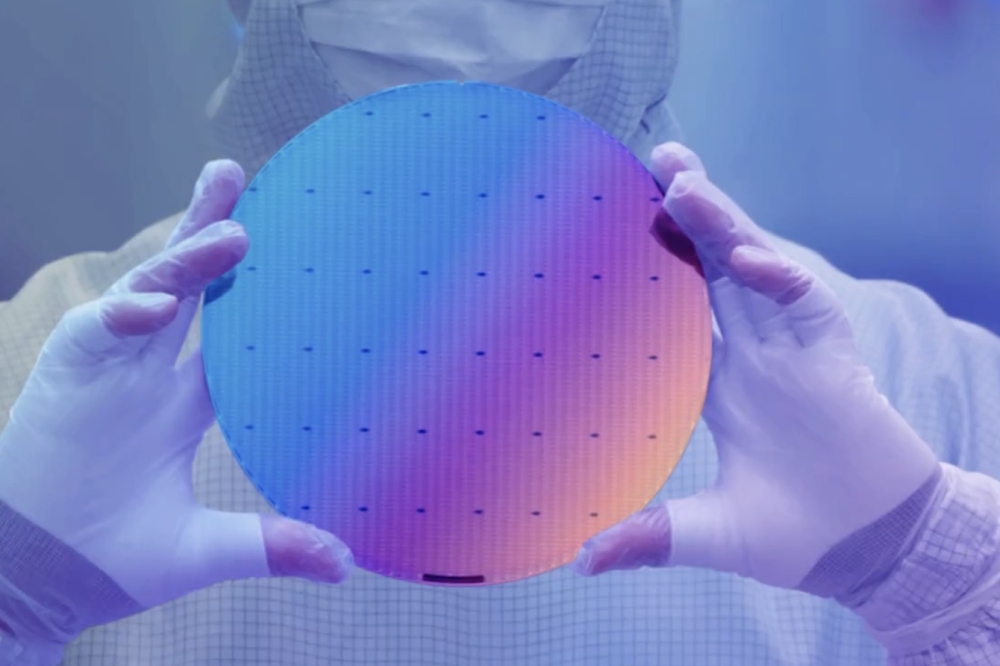
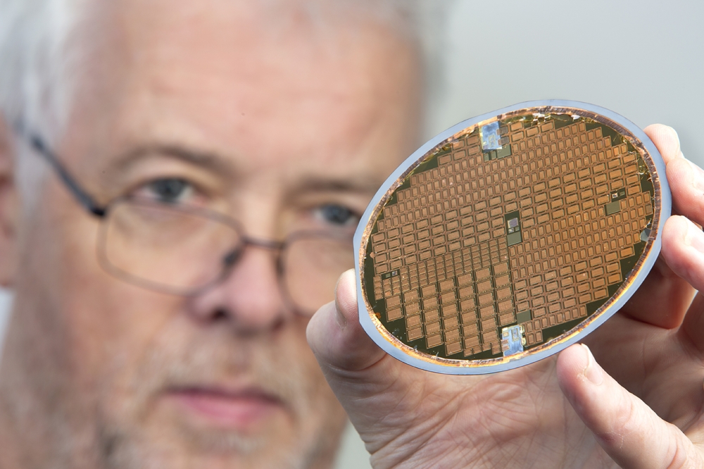
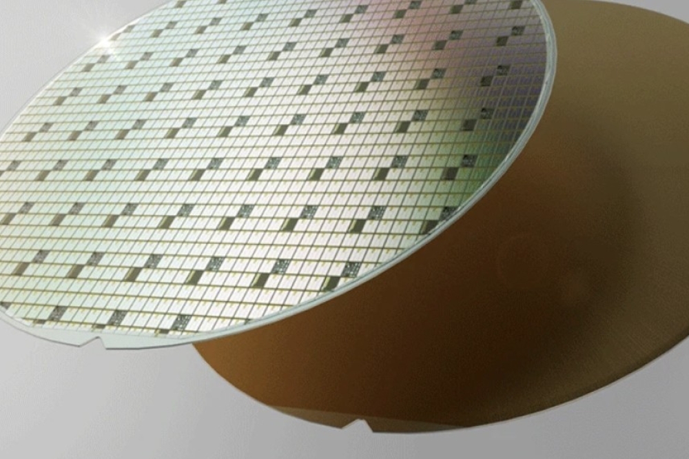
Northrop Grumman's Microelectronics centre is comprised of three manufacturing facilities – two US government-accredited semiconductor foundries in California and Maryland and an advanced packaging facility in Florida.
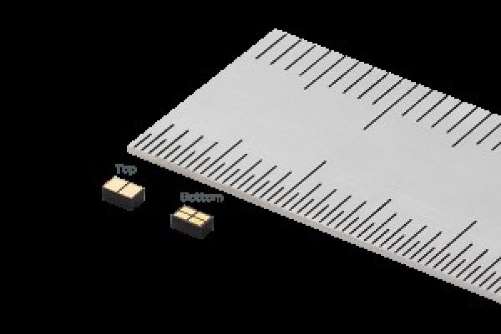
Foundry services include silicon mixed-signal, analogue, or digital ASIC’s; GaAs or GaN compound semiconductor MMIC’s; or power transistors in Silicon or SiC.
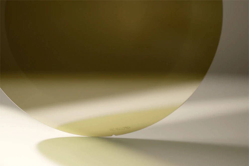
The packaging facility is capable of 100mm-300mm wafer bumping, probing, and dicing, which allows multiple smaller, specialised chips to be combined into a single, more powerful electronics package. Unlike traditional methods that place multiple chips side-by-side into a system, advanced packaging integrates multiple specialised chips together with high-density connections into a 3D chip stack.