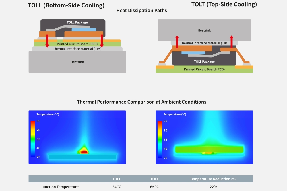
Novel annealing process improves SiC devices
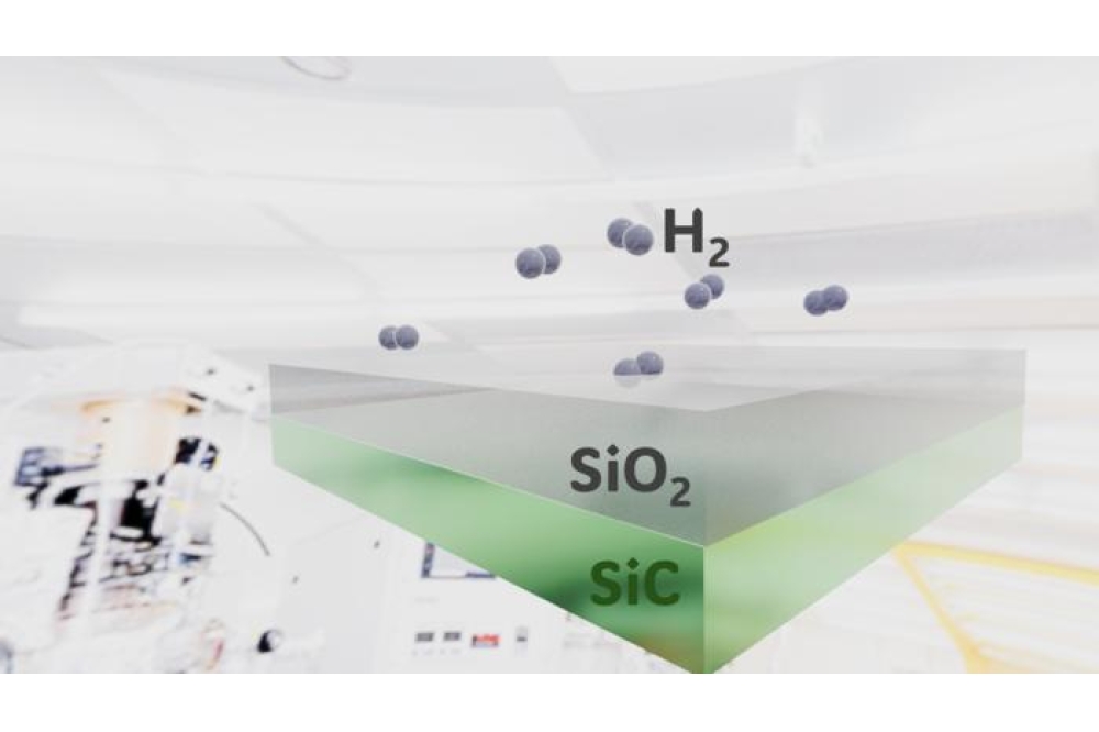
Researchers at the University of Osaka in Japan have developed a novel technique to enhance the performance and reliability of SiC MOS devices. This breakthrough uses a two-step annealing process involving diluted hydrogen, to eliminate unnecessary impurities and significantly improve device reliability.
SiC power devices offer superior energy efficiency compared to traditional silicon-based devices, making them ideal for applications like electric vehicles and renewable energy systems. However, previous attempts to improve SiC MOS device performance relied on introducing impurities like nitrogen, which unfortunately compromised reliability and limited operating voltage range. This necessitated strict gate drive design, hindering wider adoption.
The team discovered that a two-step high-temperature hydrogen annealing process, performed before and after gate oxide deposition, could drastically improve both performance and reliability without the need for these problematic impurities. This process effectively removes defects at the oxide/SiC interface, resulting in a lower interface state density and higher channel mobility. The devices demonstrated improved immunity against both positive and negative bias stress, expanding their operational voltage range.
"SiC MOS devices, despite being in mass production, haven't yet reached their full potential in terms of performance and reliability," explains Takuma Kobayashi, the lead researcher. "Our findings offer a solution to this long-standing challenge and open up exciting new possibilities for SiC power devices. We overcame many hurdles during this research, and I'm grateful to all my co-authors for their contributions."
Reference
Takuma Kobayashi et al; Applied Physics Express (2025), Volume 18, Number 8