X-FAB offers GaN-on-Si foundry services
X-FAB Silicon Foundries SE is building on its expertise in GaN processing technology for high-power applications by introducing GaN-on-Si foundry services for dMode devices as part of its XG035 technology platform.
The move builds on X-FAB’s capability as a pure-play foundry that offers a set of processing technologies for GaN and other WBG materials – including SiC – to help fabless semiconductor companies bring their designs to life.
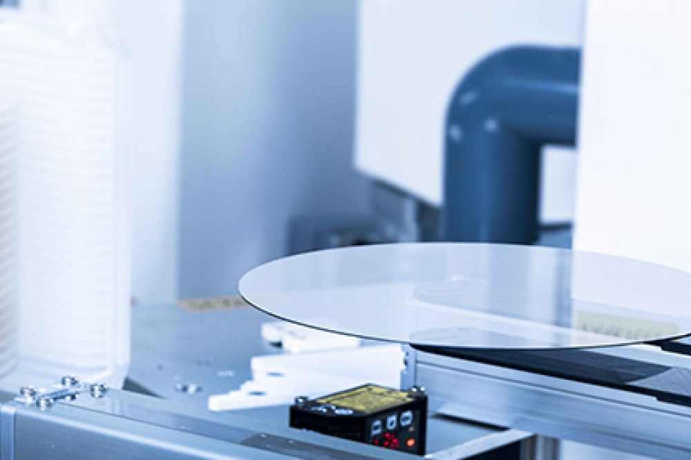
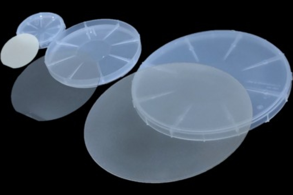
X-FAB provides the GaN-on-Si technology from its state-of-the-art 8-inch fab in Dresden, one of six production facilities operated by the company worldwide.The Dresden fab hosts specialised processing equipment, measurement tools and technologies optimised for GaN development and production, together with analog ueCMOS, in a stable, trusted, automotive-qualified fab environment.
Tools on site have also been optimised to handle the thicker GaN-on-Si wafers required by customers in sectors such as automotive, data centre, industrial, renewable energy, medical, and others, according to X-FAB.
The company’s in-house expertise now extends to GaN-on-Si foundry services for dMode devices following the recent release of its XG035 dMode technology as an open foundry platform.
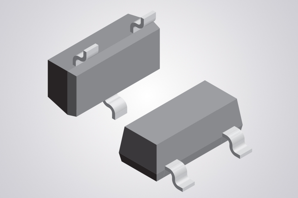
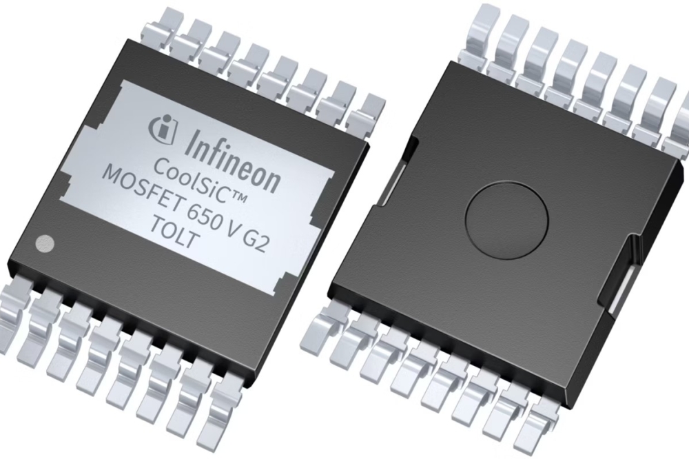
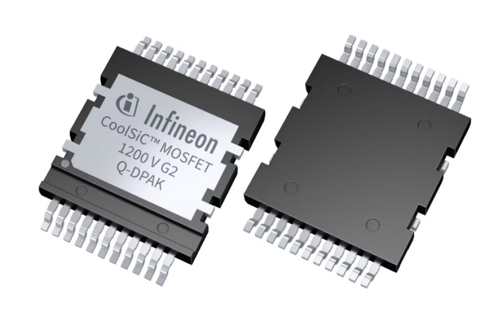
The process includes dMode HEMT transistors (scalable from 100V to 650V), often used in power conversion applications. In addition, X-FAB offers customer-specific GaN technologies including dMode, eMode HEMTs as well as Schottky Barrier Diodes, which are popular for high-frequency rectification, power supply, and solar panel applications, among others.
“Thanks to our 30+ years of experience in automotive CMOS technologies – including 350nm CMOS, shared tool sets, and shared BEOL – our GaN offering comes with built-in quality and a significantly lower barrier to entry,” explains Michael Woittennek, CEO of X-FAB Dresden. “Having developed customer-specific technologies over many years, we’re now opening up our XG035 dMode technology for general prototyping projects at our Dresden fab – in the heart of Silicon Saxony. The flexibility of our 350nm toolset also enables us to quickly scale to volume production, giving customers a fast and reliable path to market.”
“As the GaN supplier landscape evolves, X-FAB is stepping up as a dedicated GaN foundry partner,” added Luigi Di Capua, VP product marketing. “Our 8-inch GaN-on-Si platform helps customers secure their supply chain and scale their designs with confidence.”
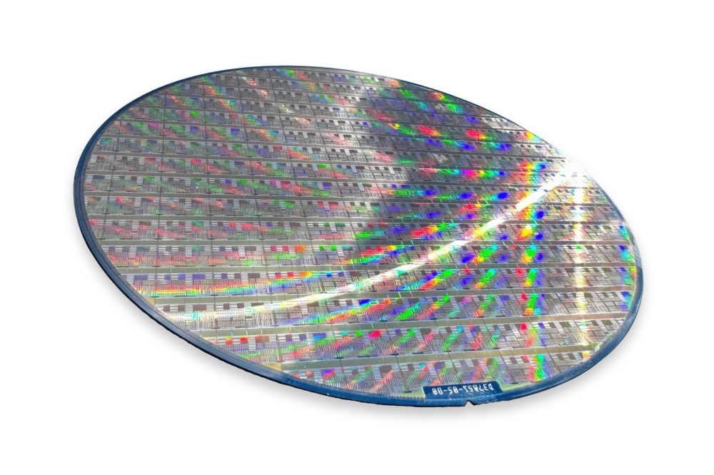
A PDK that eases the design process for customers and achieves faster on-boarding is available. In addition, a public MPW shuttle service will be available from Q4 2025, allowing multiple customers to share a single silicon wafer for chip fabrication. These steps further lower the barrier to entry for prototyping and small-volume production.