Scaling quartz-free HVPE of GaN-on-GaN epiwafers
To help increase the adoption of GaN power devices via a reduction in production costs, Sumitomo Chemical has developed a quartz-free HVPE reactor for mass production that can accommodate 6-inch substrates.
This latest triumph builds on previous successes by the Japanese company, which has shown that quartz-free HVPE can grow GaN layers with record room-temperature mobilities. Epilayers also feature very low background concentrations of silicon, oxygen and carbon.
Spokesman for the team, Ryota Ito, told Compound Semiconductor that the quartz-free HVPE technology is now very close to full optimisation. “The mobility at room temperature is close to theoretical values, and the impurity concentration is below the detection limit as measured by secondary ion mass spectrometry.”
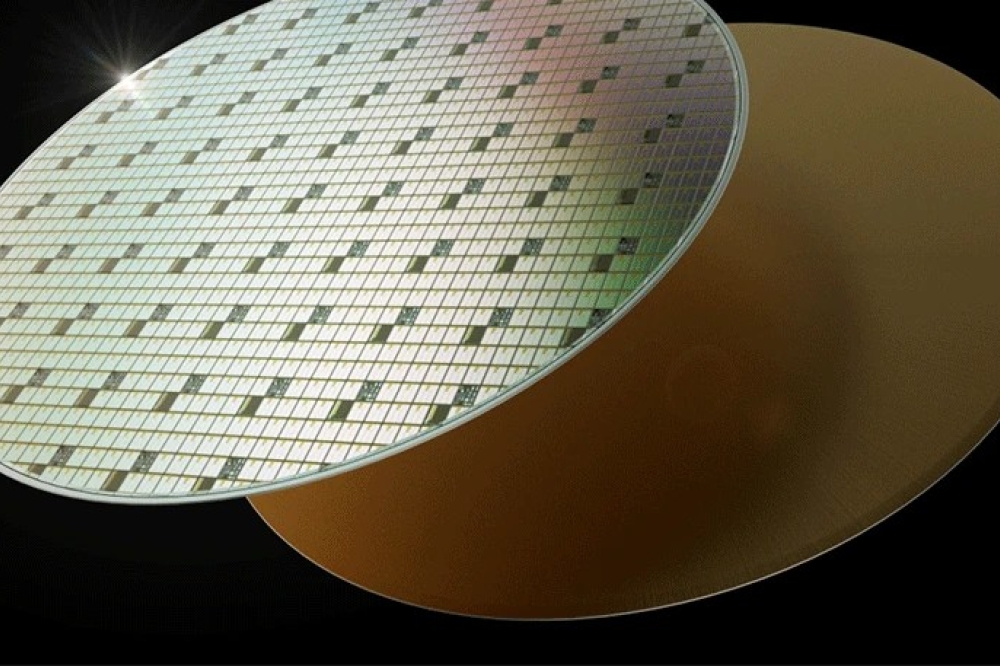
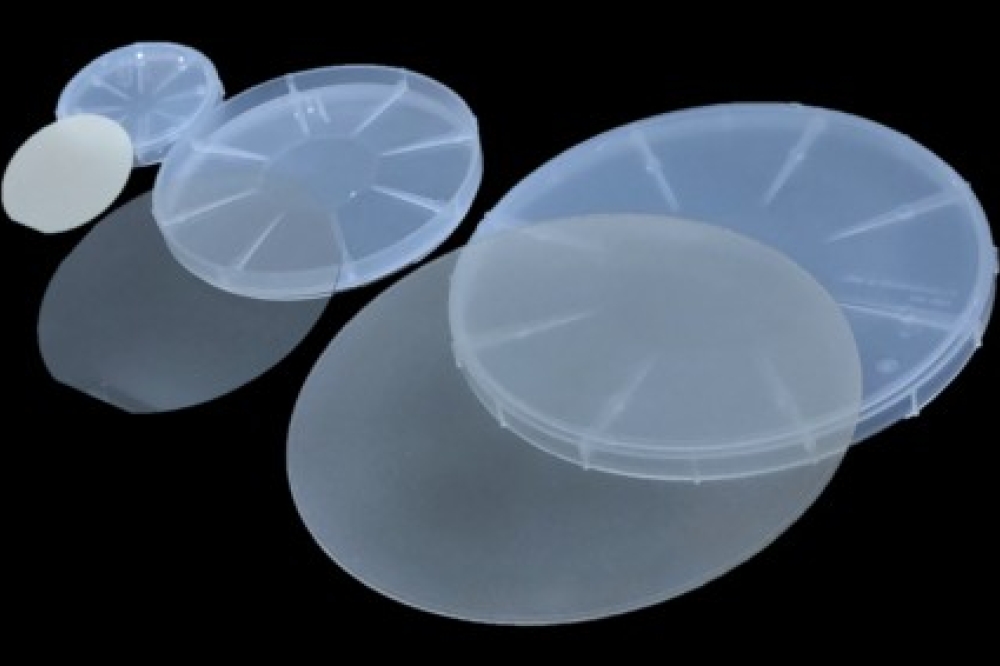
To underscore the capability of their new tool, engineers from Sumitomo Chemical have used their reactor to produce 4-inch and 6-inch GaN epiwafers. This involved the growth of a silicon-doped GaN layer, subsequently scrutinised by various characterisation techniques.
The 4-inch substrate employed in this study was produced internally, using the void-assisted separation method. This substrate had a uniform threading dislocation density of 1-3 x 106 cm-2 and an off-angle of 0.4°, tilted from the exact + c-plane towards the m-direction. “The off-cut angle is intentionally used to prevent the occurrence of hillocks,” explains Ito.
For growth on 6-inch wafers, the team at Sumitomo Chemical turned to a GaN-on-sapphire template. Note, though, that 6-inch free-standing GaN substrates are under development.
Growth conditions employed included atmospheric pressure, a growth rate of approximately 1 mm min-1, the use of ammonia and gallium monochloride as source gases, and a mixture of hydrogen and nitrogen for the carrier gas.
According to Fourier transform infrared spectroscopy, the silicon-doped GaN epilayer on the 4-inch native substrate has a thickness of 14.1 mm, with a standard deviation of 3.4 percent. Commenting on this, the team remarked in their paper that whereas conventional HVPE-grown GaN tended to exhibit a large thickness variation, the optimised quartz-free HVPE system led to a uniform distribution, similar to that of an MOCVD-grown epitaxial film.
For the growth of epiwafers on 6-inch templates, the thickness uniformity is a little higher, with a standard deviation of 4.4 percent.
To evaluate doping, the engineers at Sumitomo Chemical considered the difference between the density of donors and acceptors, determined by a non-contact capacitance-voltage instrument. For MOCVD-grown GaN on 100 mm free-standing GaN, the standard deviation is 14.3 percent – and for GaN grown by quartz-free HVPE on 100 mm free-standing GaN it’s just 3.0 percent.
The team also conducted photoluminescence measurements on their latest GaN epilayers, and compared the spectra with that obtained for an equivalent sample produced with a prototype reactor. The film grown with the more recent reactor, designed for mass-production, produces stronger near-band-edge emission, thanks to suppression of carbon contamination. Also encouraging is a reduction in green luminescence, indicative of a reduction in the density of point defects – this is attributed to a superior reactor design that supresses the leakage of gas from/into the growth area.
To demonstrate carrier control in their quartz-free HVPE reactors, the engineers at Sumitomo Chemical varied the silicon source rate, with a step change for every 600 nm of GaN growth. Analysing the doping profile via secondary ion mass spectrometry determined that the doping level is constant in each layer, and at the interfaces there is a steep change in silicon concentration.
This investigation also showed that with the latest quartz-free HVPE reactor there is linear doping with silicon concentration, over a wide range from 1 x 1014 cm-3 to 1 x 1018 cm-3.
As many power devices operate in the kilovolt range, controlling the carrier concentration in the range below 1 x 1016 cm-3 is critical. Excelling in this regard, Sumitomo Chemical’s latest quartz-free HVPE reactor offers the capability to produce devices with breakdown voltages of 10 kV or more.
Sumitomo Chemical does not intend to produce and sell its quartz-free HVPE reactors. “We are a GaN substrate vendor, and we are planning to sell GaN-on-GaN epitaxial wafers produced by quartz-free HVPE,” says Ito.
Today, Sumitomo Chemical is selling its GaN substrates with diameters of up to 4 inches, and is providing epitaxial wafers grown by quartz-free HVPE to device manufacturers and research institutions.
“Furthermore, we are developing 6-inch GaN substrates, and will soon be able to offer 6-inch GaN-on-GaN wafers,” says Ito, adding: “Through this, we aim to contribute to the early establishment of the vertical GaN device market.”
Reference
S. Kaneki et al. Appl. Phys. Express 18 055502 (2025)