A GaN-on-silicon foundation for Ga₂O₃ FETs
Engineers from King Abdullah University of Science and Technology are claiming to have unveiled the first Ga2O3 transistors grown on GaN-on-silicon.
According to these researchers, turning to this particular form of heterogeneous integration allows the Ga2O3 transistor to retain its strengths, including a very high breakdown field that makes it a very promising device for power electronics, while potentially addressing its weaknesses – it is held back by a low thermal conductivity and inefficient p-type doping. What’s more, this combination of materials could open the door to large-scale manufacturing.
When considering the various material options for underpinning the Ga2O3 transistor, the team dismissed SiC. While this substrate has a high thermal conductivity, it is expensive and incompatible with silicon process technology, hampering monolithic integration
The team from Saudi Arabia view their combination of a Ga2O3 transistor, a GaN buffer, and a silicon substrate as a compelling one, because it is more scalable, more cost-effective, and it avoids compromising performance.
By adopting this approach, devices benefit from the strengths of GaN, including its high thermal conductivity. In addition, according to team spokesman Xiaohang Li, it’s possible that p-type GaN might be able to tackle the poor p-type doping in Ga2O3.
Another asset of this combination is that it could create monolithic ICs that feature: high-speed control circuitry, drawing on the superior mobility of GaN; and high-power devices, produced from Ga2O3.
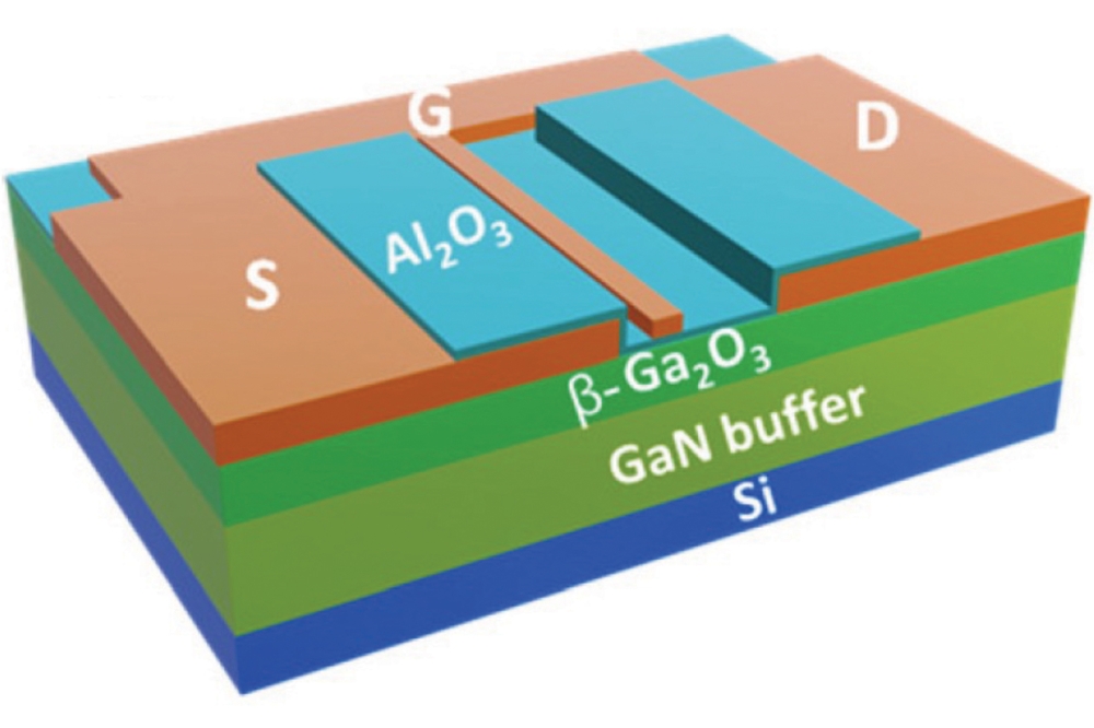
To fabricate their devices, Li and co-workers began by using pulsed laser deposition (PLD) to grow a roughly 50 nm-thick film of silicon-doped Ga2O3 on a semi-insulating 4.7 µm-thick GaN buffer layer.
Explaining this choice of growth technology, Li remarks: “PLD has proven to be a viable tool to grow high-quality epitaxial Ga2O3. MOCVD may offer moderately better materials, but MOCVD is not as compatible to the silicon CMOS process as PLD.”
Electrical measurements determined that the film of Ga2O3 has an electron concentration of around 1.2 x 1018 cm-3, and a mobility of just 2.1 cm2 V-1 s-1. Low mobility is attributed to the polycrystallinity of the Ga2O3 layer and defects induced by lattice mismatch.
It’s claimed that mobility can be increased by adopting advanced growth techniques, such as MOCVD, and applying post-growth high-temperature annealing, which enhances crystallinity and reduces defect density.
To fabricate devices, Li and co-workers added source and drain Ti/Au terminals to their epistructure, before depositing a 25 nm-thick Al2O3 gate dielectric by atomic layer deposition, adding a gate metal, and then using reactive ion etching to open up source and drain pads. Transistors produced with this process have a gate length of 4 µm, a source-to-gate separation of 3 µm, and a gate-to-drain distance of 18 µm.
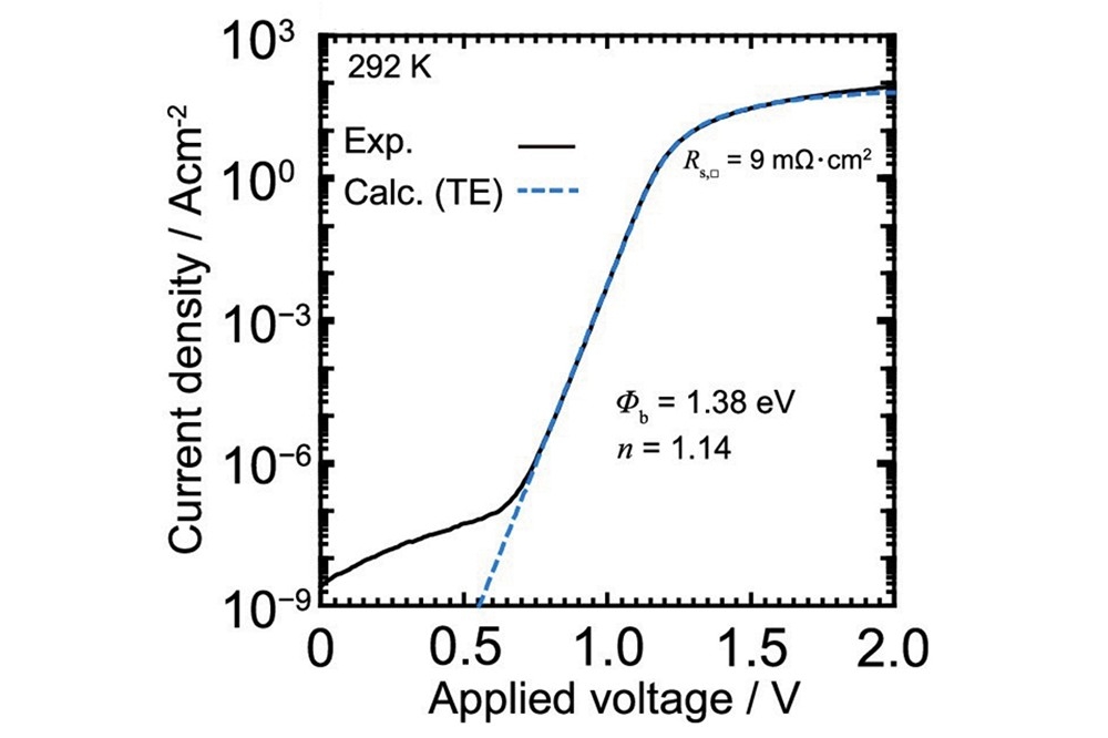
Electrical measurements on these devices enabled the team to calculate a sub-threshold swing of 167 mV dec-1 – a value that indicates a high-quality interface between Ga2O3 and Al2O3 – and determine an on-off ratio of around 106. At a gate-to-source voltage of 8 V, the off-state gate leakage current is around 10-7 mA mm-1, and at a drain-source voltage of 5 V the threshold voltage is 3 V, enabling fail-safe operation.
The breakdown voltage, measured at a gate-source voltage of 0 V, has a maximum value of around 540 V. According to the team, this is the highest value for b-Ga2O3 MOSFETs on silicon substrates.
One alternative to the team’s b-Ga2O3 MOSFETs on GaN-on-silicon substrates are variants produced on AlN-on-silicon. Earlier this year, such devices were reported by a collaboration led by researchers at National Chung Hsing University.
“That’s a very nice work,” says Li. However, he argues that there are a number of issues with b-Ga2O3MOSFETs on AlN-on-silicon, including a rough surface morphology, depletion-mode operation, and a lower breakdown voltage.
“In addition, AlN-on-silicon is prone to cracks, and it is not as mature as GaN-on-silicon as a platform,” adds Li. However, he believes that with more development, it is possible that AlN-on-silicon can become a good platform.
Li says that the next goals for the team include developing various power technologies associated with Ga2O3-on-silicon, through the use of GaN, as well as integration with p-GaN.
Reference
M. Kumar et al. Appl. Phys. Lett. 126 193505 (2025)