Debut for vertical rutile GeO₂ Schottky barrier diode
Researchers from Kyoto Institute of Technology are claiming to have broken new ground by demonstrating the first vertical rutile GeO2 Schottky barrier diode (rutile GeO2 is a tetragonal crystal structure, where Ge4+is bonded to six equivalent O2- atoms to form a mixture of corner and edge-sharing GeO₆ octahedra).
Putting this success in context, team spokesman Hiroyuki Nishinaka remarked: “While a Japanese venture company has shown a pseudo-vertical Schottky barrier diode on their website, it has not been published in a peer-reviewed journal with detailed information.”
Nishinaka added: “While other groups have reported GeO2 photodetectors, our work represents the first vertical power device demonstration.”
Like its cousin, Ga2O3, rutile GeO2 has an ultra-wide bandgap that ensures a high critical electric field, and makes this oxide a promising material for producing power devices.
But in addition to this similarity, rutile GeO2 has several advantages over Ga2O3. Most notably, theoretical work suggests that rutile GeO2 can doped both n-type and p-type.
According to these calculations, despite relatively high acceptor ionisation energies, co-doping strategies have the potential to increase acceptor solubility to enable hole conduction through an impurity band. “In contrast, b-Ga2O3 faces significant challenges with p-type doping due to its intrinsic material properties, and has not been successfully p-type doped to date,” argued Nishinaka
He and his co-workers have produced vertical rutile GeO2 Schottky barrier diodes on niobium-doped TiO2substrates, as native substrates are not commercially available.
“However, researchers at IKZ in Germany have reported highly conductive antimony-doped bulk rutile germanium oxide, suggesting that native substrates suitable for power device applications may become available in future.”
The team used mist-epitaxy to deposit their epistructure at 850 °C. This consisted of an antimony-doped, graded GeySn1-yO2 buffer layer and
an unintentionally doped rutile GeO2 layer.
“We use mist CVD for growth because I am one of the researchers who developed mist CVD at Kyoto University, so we have extensive expertise with this technique,” explained Nishinaka. “Mist CVD has particular advantages in early-stage materials research because it can utilise any material that can be dissolved in solution. While MOCVD is also suitable – and has been used to grow rutile germanium oxide – mist CVD offers advantages in materials exploration.”
Secondary ion mass spectrometry has revealed that the buffer is 149 nm-thick and the GeO2 layer has a thickness of 198 nm. This technique also determined that antimony diffuses from the buffer into the GeO2layer, possibly due to defect-assisted diffusion mechanisms, such as dislocations or point defects.
After cleaning the samples, the team turned to evaporation to add nickel Schottky contacts with a diameter of 320 nm.
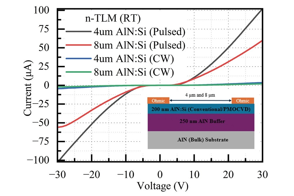
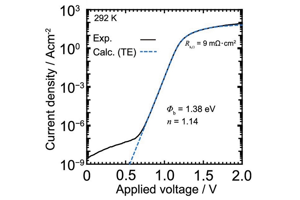
Electrical measurements determined: clear rectifying behaviour, with a rectification ratio of 6 x 10⁵ at ± 2 V; an on-resistance of 9 mΩ cm2, a value that is consistent with the resistance of the substrate; an ideality factor of 1.14; and a Schottky barrier height of 1.38 eV.
One of the weaknesses of the Schottky barrier diode is its relatively high reverse-leakage current, possibly due to a leakage path.
According to the team, improvements in epitaxial growth are needed to determine whether the reverse leakage current mechanism in ideal rutile GeO2 can be accurately described by the thermionic emission model, which has already been successfully applied to 4H-SiC, GaN and b-Ga2O3.
Progress with rutile GeO2 also hinges on reducing dislocations and/or point defects and realising uniform doping control in thick epilayers.
“Our next goals focus on achieving reliable p-type doping to realise p-n junction devices, ultimately leading toward MOSFET development for rutile germanium oxide,” remarked Nishinaka.
Reference
K. Kanegae et al. Appl. Phys. Express 18 041001 (2025)
Pictured above: Forward current-voltage characteristics of the vertical rutile GeO2 Schottky barrier diode, showing clear rectification behaviour