Pulsed MOCVD improves n-type AlN
One of the weaknesses of AlN, which hampers its deployment in high-power and high-temperature electronics, is its limited n-type conductivity when grown by MOCVD. But this drawback can be overcome by moving to migration-enhanced pulsed MOCVD, according to engineers from the University of South Carolina and Texas Tech University.
Tariq Jamil from University of South Carolina told Compound Semiconductor that as well as the introduction of pulsed MOCVD, a well-established technique, n-type conductivity benefits from the use of low defect-density substrates and pseudomorphic growth. “This removes any complications in doping measurements from the extended defects that are common in hetero-epitaxial growth,” argues Jamil, who adds it is also important to carefully optimise the growth temperature and the dopant concentration for each pulse to avoid over-doping, which can lead to compensation.
Jamil and co-workers have demonstrated the merits of pulsed-MOCVD by comparing silicon-doped AlN layers produced by this technique with those grown by its conventional counterpart.
For this investigation, the researchers cleaned c-orientated AlN substrates with organic solvents, before loading them into an MOCVD chamber and annealing them under ammonia at 1150 °C. After growth of a 200 nm-thick undoped AlN layer at 1150 °C using conventional MOCVD, the team added a 200 nm-thick n-type AlN layer at the same growth temperature, producing samples by both conventional MOCVD and pulsed MOCVD. For the latter process, the introduction of the silicon-dopant coincided with a pulse of the aluminium-based precursor.
Characterisation revealed high material quality. Atomic force microscopy determined very smooth surfaces, with root-mean-square values for surface roughness of 0.92 nm and 0.42 nm for n-type epilayers grown by conventional and pulsed MOCVD, respectively. High-resolution X-ray diffraction produced linewidths for the off-axis (1012) and on-axis (0002) of below 40 arcsec for n-type AlN produced by both forms of MOCVD, enabling estimates for dislocation densities in this layer of around 103 cm-2.
Pumping samples with a 193 nm laser provided photoluminescence spectra, featuring a peak at 5.93 eV, due to emission from the AlN band edge. The sample produced by pulsed MOCVD has a more intense peak, attributed to higher-quality material.
Another feature in the photoluminescence spectra is a peak at 3.2 eV, associated with aluminium-vacancy formation that results from silicon doping. According to the team, the significant difference in conductivity between the two samples cannot be explained by the aluminium-vacancy/silicon complexes, and might result from a reduction in point defects. To look into this, the team is now undertaking low-temperature photoluminescence measurements.
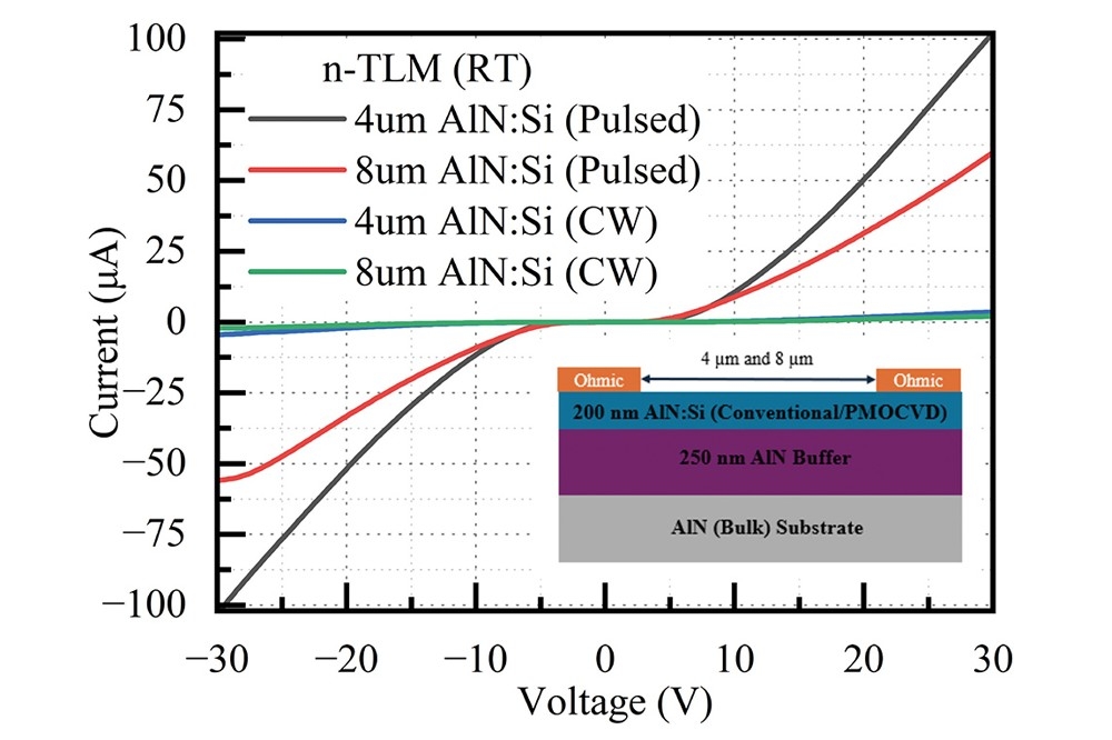
Jamil and co-workers have already investigated the conductivity of their samples with the transmission-line method, adding ohmic contact metals spaced 4 µm and 8 µm apart and annealed at 950 °C for 30 s. Current-voltage plots are non-linear at low currents (see figure), hampering estimates of contact resistance. What is clear, though, is the superior conductivity of the sample grown by pulsed MOCVD, which produces a current at a 25-volt bias exceeding that of its conventional counterpart by more than an order of magnitude.
Undertaking current-voltage plots at a range of temperatures has enabled the team to estimate the donor ionisation energy for silicon in AlN. The value obtained is around half that reported by other groups, suggesting pulsed MOCVD leads to a different mechanism for silicon incorporation.
Optimising the growth process is still a work in progress, according to Jamil: “Pulse growth mode has a lot more knobs one can turn. They include aluminium and ammonia pulse widths, metal-organic/dopant concentration in the pulse, temperature, and pressure.”
Over the coming months, the team expects to report additional progress in its pulsed-mode growth technology, and to start investigating new dopants, such as germanium for n-type doping.
Pictured above: Pulsed-mode MOCVD is far better at producing silicon-doped AlN layers than conventional MOCVD, according to current-voltage transmission line measurements using electrodes with 4 µm and 8 µm spacings.
Reference
T. Jamil et al. Appl. Phys. Express 18 025501 (2025)