GaN companies strengthen patent portfolios
KnowMade has published its Q1 2025 IP report on GaN electronics, highlighting robust patenting activity across both power and RF segments, amid on-going patent disputes between power GaN companies.
Recent patent filings emphasise critical aspects of power GaN technology such as gate design and packaging, resulting in sustained patent portfolio growth. Meanwhile, key RF market players keep expanding their IP activities in the RF GaN landscape, underlining the technology’s role in next-generation wireless applications.
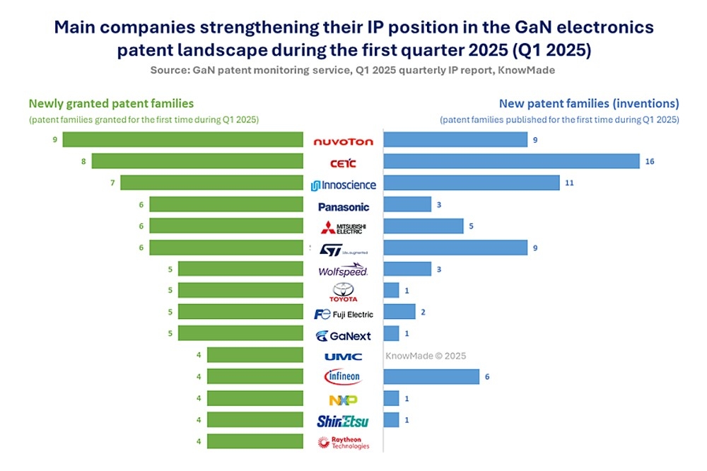
During the first quarter of 2025, a total of 540 new patent families were published, with Xidian University and major Chinese entities such as CETC and Innoscience leading the patent filings, followed by contributions from Nuvoton, STMicroelectronics, and Toshiba. Over 330 patent families were granted for the first time, notably reinforcing portfolios at Innoscience, STMicroelectronics, Infineon, Navitas, and EPC, alongside significant grants to Panasonic and TSMC. The quarter also saw more than 110 patents abandoned and over 70 patents expired, primarily from well-established patent holders including Wolfspeed, Infineon, and Fujitsu.
Approximately 10 IP collaborations (patent co-filings) were recorded, most partnerships formed between industry and academic organisations. For instance, Safran published a patent application with CNRS, CNAM and several universities in Paris, for an on-board aeronautical power circuit with active filtering. Also, Volkswagen cooperated with the University of Tennessee on GaN-based three-level active neutral point clamped power module designs, resulting in joint patent publications in Q1 2025.
Nearly 40 patent transactions took place this quarter, predominantly within China, such as the transfer of several RF GaN patents from Xidian University to Huawei and power module company Macmic Science & Technology’s acquisition of a GaN device patent from UESTC.
In addition, a new lawsuit was initiated in February 2025 when Innoscience appealed to the US Court of Appeals to challenge the US International Trade Commission’s ruling in last November on EPC’s patent US 8,350,294.
Top Innovators in Power GaN
Toshiba, Texas Instruments (TI), and Rohm each published more than six new inventions. In particular, Rohm introduced multiple innovations aimed at enhancing the reliability of normally-off GaN devices by leveraging p‐GaN gate layer techniques and superlattice buffer structures. TI unveiled a novel gate structure incorporating a p‐type poly‐Si layer to decouple parasitic capacitances and improve gate depletion behavior, alongside trench-based substrate-to-source connections for GaN power devices and a HEMT design featuring a doped barrier to boost threshold voltage stability and drain current stability. Moreover, TI disclosed a packaging solution wherein a GaN FET is co-packaged with its driver for optimised half-bridge modules.
Leading RF GaN Developments
Sony, Sumitomo Electric, and Macom disclosed six, five, and four RF-focused inventions, respectively. While Sumitomo Electric and Sony were focused on RF GaN device designs, Macom’s patenting activity related to RF amplifier circuitry and advanced packaging techniques.
Interestingly, Sumitomo Electric focused on RF GaN-on-SiC devices fabricated on nitrogen-polarity GaN epitaxial structures. Academic research also made a significant contribution on this topic with UCSB publishing an invention that improves the linearity of deep-recess GaN MIS‐HEMTs through corrugation of N-polar structures. MONDE Wireless, a UCSB spin-off, also mentioned N-polar GaN HEMTs grown on miscut substrates in another Q1-2025 patent publication.
Emerging players
New entrants to the GaN electronics IP landscape were predominantly Chinese, with LED manufacturer Anhui GaN Semiconductor filing several epiwafer patent applications for both power and RF uses, and battery manufacturer CATL submitting its first GaN-related invention targeting battery management systems. In the US, Tesla entered the arena with a packaged integrated circuit device featuring enhanced power surge heat dissipation, and Soctera, a Cornell University spin-off, proposed a GaN device structure using an AlN back barrier layer and in-situ two-step passivation process to mitigate current collapse.