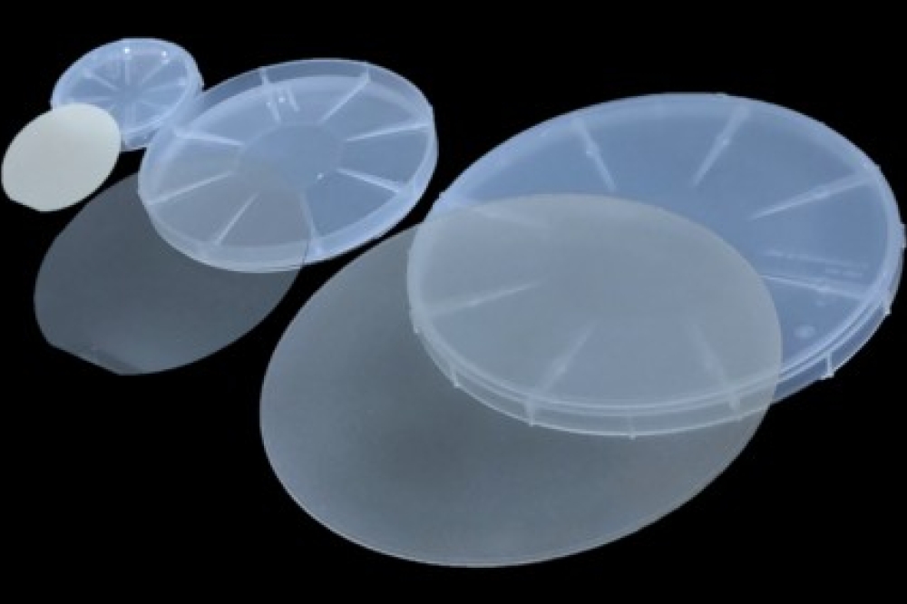
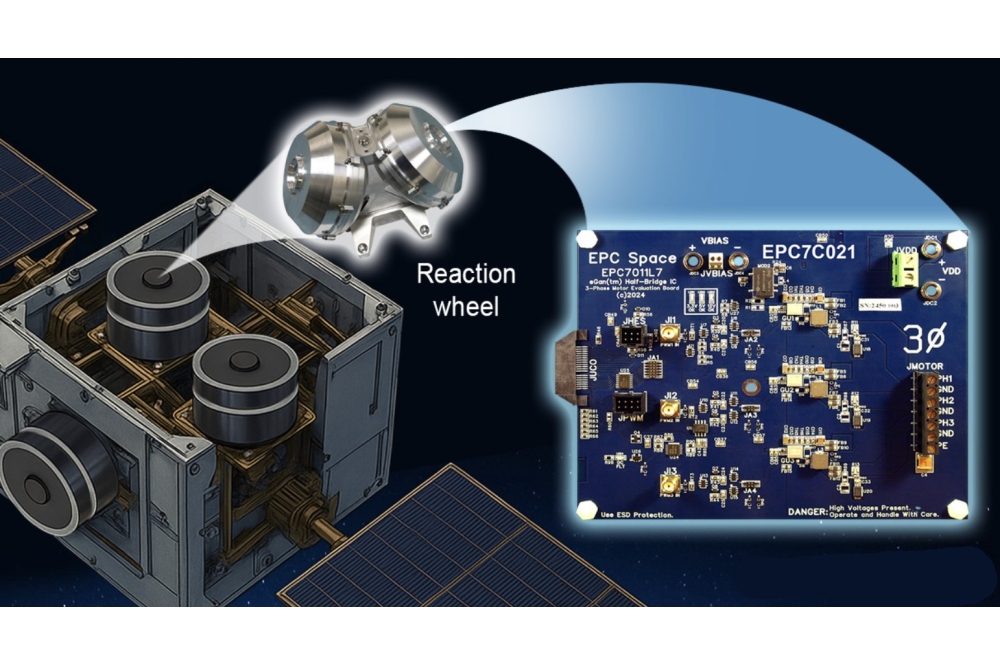
A*STAR launches 200mm SiC open R&D line
Singapore's Agency for Science, Technology and Research (A*STAR) hosted the inaugural 'Innovate Together' event at SEMICON Southeast Asia 2025, while announcing the World’s first industry-grade 200mm SiC Open R&D Line.
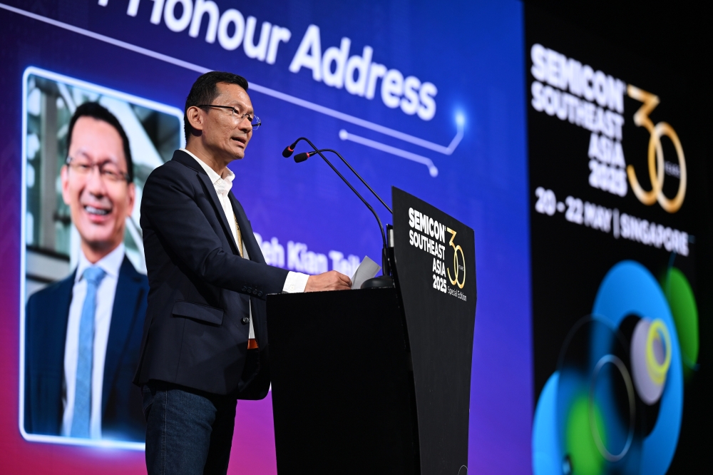
"Singapore's semiconductor ecosystem is built on strong collaborations between public agencies, academia, and industry partners," said Yeo Yee Chia, deputy chief executive (Innovation & Enterprise) at A*STAR. "The Innovate Together event exemplifies our commitment to fostering these partnerships and accelerating innovation to address industry challenges and capture new opportunities in the global semiconductor landscape."
At the heart of Innovate Together was the launch of the SiC Open R&D Line. Designed to enable joint SiC innovation between researchers and companies, the aim is for the facility to strengthen Singapore's capabilities in wide bandgap semiconductor research and address the future demands for high-power applications.
In addition, A*STAR unveiled two other initiatives to strengthen Singapore’s semiconductor research and innovation capabilities:
- Phase two of Lab-in-Fab, a 200mm R&D and manufacturing line focused on piezoMEMS, involving partners STMicroelectronics, ULVAC, and the National University of Singapore. This will build on Singapore’s strong R&D ecosystem to accelerate the development of new piezoelectric materials and devices.
- EDA Garage, an initiative that will provide local companies, especially start-ups and SMEs, with cost effective access to advanced Electronic Design Automation (EDA) tools. This will nurture local semiconductor companies and enable them to innovate faster and better.
To kickstart international collaborations in semiconductor training and R&D, A*STAR IME signed Memorandums of Understanding (MOUs) with key partners, including the Uzeltexsanoat Association, representing Uzbekistan’s electronics sector, the Singapore Semiconductor Industry Association (SSIA), the Indian Institute of Technology, Kharagpur (IIT KGP), and the Fraunhofer Institute for Electronic Nano Systems ENAS.
These partnerships pave the way for internship programmes, joint research projects, and knowledge exchange through training and knowledge sharing activities.
At the sidelines of the SEMICON Southeast Asia 2025 event, A*STAR also formalised its partnerships with GlobalFoundries and Nearfield Instruments, to expand capabilities in advanced packaging and drive innovation in semiconductor metrology technologies.
Under an MOU, GlobalFoundries will gain access to A*STAR’s advanced R&D facilities, capabilities and technical support for technology development in advanced packaging and workforce skills enhancement. The multi-year research collaboration between A*STAR IME and Nearfield Instruments will accelerate the development of advanced metrology solutions that enable efficient chip production.
The Innovate Together event featured expertise from other institutions on key technological areas that are important for the future of Singapore’s semiconductor industry. Speakers from A*STAR, National University of Singapore (NUS), Nanyang Technological University, Singapore (NTU Singapore), and the National Semiconductor Translation and Innovation Centre (NSTIC) shared the latest insights on advanced packaging, photonics, MEMS, and mmWave and beyond.