Dynamic characterisation of a power semiconductor bare chip
Power semiconductor devices are used in a variety of forms, such as being packaged in Surface Mount Devices (SMDs) or power modules, and they find broad applications.
by Keysight
Power semiconductor bare chips are loaded into these packages. It is desirable to characterize the bare chip before placing it in a package or a power module to expedite development. However, the small size, fragile structure, and parasitic effects caused by probing create multiple challenges for dynamically characterizing these power semiconductor bare chips. This article reviews the challenges of performing dynamic characterization on a bare chip, as well as some new technologies that help address these challenges.
Do you have a desire to measure power semiconductor devices as soon as they are fabricated? Power semiconductor devices are initially fabricated on a wafer, followed by dicing and packaging before they can be used in actual power electronics circuits. Characterization in the early phases of the manufacturing process helps expedite device development. For power module development engineers, understanding the behavior of power semiconductor bare chips is beneficial for accelerating development and aiding in troubleshooting.

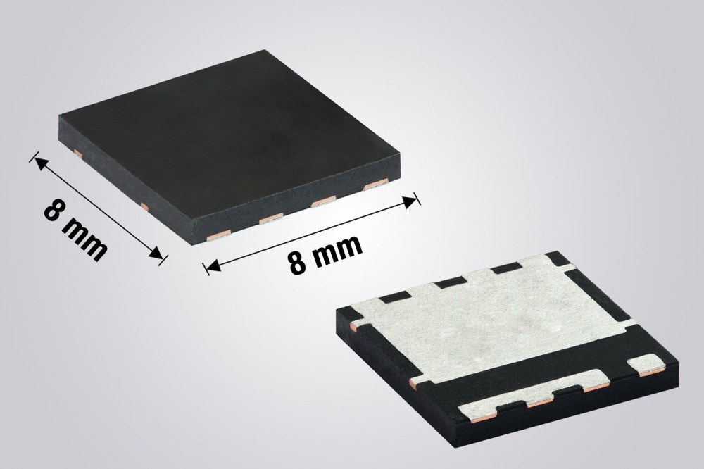
Figure 1. Example bare chip (courtesy of Wolfspeed)
Challenges for dynamic characterization on power semiconductor bare chips
Static characterization of power semiconductor bare chips is not too difficult. The chip is physically fixed tightly on an electrically conductive stage for drain contact, and the source and gate are probed using needles from the top side of the chip. Parasitics associated with the fixturing do not significantly deteriorate measurement performance. Instruments such as curve tracers or impedance analyzers can be used for static characterization.
On the other hand, dynamic characterization of power semiconductor bare chips is extremely difficult. First, parasitics in the test circuit significantly deteriorate dynamic characterization, especially for Wide Band Gap (WBG) power semiconductors due to their fast speed. For instance, probe needles introduce additional parasitics, causing oscillation, ringing, and resulting in distorted measurement waveforms. These probe needles can also pose a risk of arcing due to the high voltage signals used in testing.
Second, SiC MOSFETs, vertical GaN devices, Si MOSFETs, and IGBTs have a vertical device structure where the current flows from the top of the chip to the bottom. Probing a chip from both the top and bottom is extremely challenging. Therefore, one side of the chip must be soldered. However, soldering and unsoldering the chip to a PCA (Printed Circuit Assembly) is inconvenient and accelerates board wear, making it less than ideal for testing.
Third, bare chips are physically fragile. Unbalanced forces during fixturing can easily cause cracks or chipping. Additionally, the small size of the chip — often less than 5mm on one side — makes handling even more difficult.

Figure 2. Example PD1500A DUT board for dynamic characterization of a bare chip.
Fourth, bare chips can break due to voltage surges caused by the fast di/dt (rate of change of current) of the test signal, coupled with surrounding parasitic inductance.
The only method currently used to characterize a bare chip is to create a complete Double Pulse Test (DPT) board for the chip. This board includes an integrated PCA with gate drivers, bank capacitors, isolation components, and other necessary elements. The chip is soldered to the PCA on the drain side, and wire bonding is used to establish connections to the source and gate. Often, the chip is coated with insulating material. However, this setup is employed only once for chip characterization because the PCB cannot be reused. The associated costs, time, effort, and lack of reusability discourage engineers from using it frequently.
Technologies enabling dynamic characterization of a bare chip
There are a few key technologies and know-how that are necessary to enable dynamic characterization of a bare chip. The creation of a special fixture for a bare die is the most important aspect of the solution. This special fixture must meet the following requirements:
• No probing needle should be used to avoid extra parasitic effects and the risk of arcing.
• The fixture must make contact with the vertical structure of the bare chip.
• Contact with the bare chip must be tight enough to ensure electrical conductivity but not too tight to avoid physical cracks or chipping.
• Solderless contact is desirable.
• A mechanism is needed to align a small bare chip with the electrodes on the test fixture.
• Parasitic effects in the test fixture should be minimized (e.g. < a few nH)
• The fixture should have high voltage and high current capabilities (e.g., 600 V and 40 A)
Additionally, there are several know-how techniques to accomplish this difficult task. For example, handling a bare chip gently is essential to avoid physical damage.

Figure 3. Tailored bare chip DUT fixture for PD1500A/PD1550A.
A solution for dynamic characterization of a bare chip
Keysight has two double pulse test systems: one is the PD1500A for discrete power devices, and the other is the PD1550A for both discrete power devices and power modules. The solution described below utilizes newly developed technologies for chip dynamic testing and is realized for the PD1500A. The DUT board is rather simple, as shown in Figure 2. The same technology can be leveraged for the PD1550A, allowing power module engineers to use it for characterizing bare chips and power modules with this new solution.
In the DUT board, special treatments are applied to the electrodes on the PCB to allow solderless contact. A flexible PCB with a similar electrode treatment is also used for top-side connections. By placing a chip between the main PCB and the flexible PCB, it becomes possible to flow current from the top of the chip to the bottom, enabling current measurements for vertical structure
devices.
The PCB design aims to minimize parasitic inductance in both the power loop and gate loop. The fixture features carefully designed multiple pins protruding from the PCA, which align a bare chip precisely for optimal contact with the electrodes. The absence of probe needles further reduces parasitic inductance in the test circuit.
For Si and SiC devices, a coaxial shunt resistor can be used, even with its several nanohenry (nH) range of extra insertion inductance. In the case of GaN (Gallium Nitride) bare chips, Keysight’s patented current sensor 1 provides an additional means to minimize parasitic inductance.

Figure 4. Test results (turn-on & turn-off) for a SiC MOSFET.
Power semiconductor bare chips typically exhibit different form factors. Therefore, our strategy involves creating a customized DUT board for both the PD1500A and PD1550A, as illustrated in Figure 3.
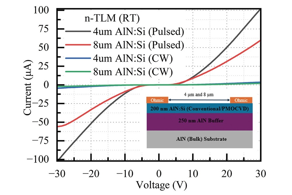
Figure 4 shows example measurement results taken for a 1.2 kV-rated SiC MOSFET bare chip. The test is performed at 800 V and 40 A, demonstrating that the fixture provides sufficient voltage and current capability for the 1.2 kV-rated SiC MOSFET. The waveforms are very clean, with a small Vds overshoot at turn-off. The calculated power loop inductance from the turn-on waveform is only 8.3 nH.
The fixture for bare chips can also be easily used with curve tracers such as the Keysight B1505A/B1506A. It eliminates the need to use a wafer prober for bare chip static measurements, greatly improving productivity.
Summary
Bare chip dynamic characterization, once regarded as very challenging and almost impossible to do, is now available through newly developed solution for Keysight PD1500 series double pulse testers. It is provided as tailor-made solution for a bare chip. There are many know-hows associated with the solution to perform the test safely and with minimized risks. For more information, contact your local Keysight representative.