Power-SOI technology and its potential to shape the future of power electronics

Soitec’s Power-SOI 300mm substrates for advanced gate driver ICs to drive power conversion wide-bandgap devices at high switching frequency. This feature examines Power-SOI technology and its potential to shape the future of power electronics, paving the way for more efficient, compact systems across automotive, industrial, and renewable energy sectors.
By Alex Lim and Rainer Lutz, Soitec
The power electronics industry continues to pursue higher efficiency, greater power density, and better thermal management. With silicon-based IGBTs reaching their limits, WBG semiconductors like SiC and GaN are emerging as leading options for next-generation applications.
Although WBG materials offer superior properties, fully leveraging them requires specialized driving and control solutions. This white paper introduces Power-SOI technology, designed to unlock the full potential of WBG devices in power conversion and motor control systems.
Figure. 1 GD3162 Efficiency Gain with Dynamics GS (Courtesy to NXP Semiconductors)
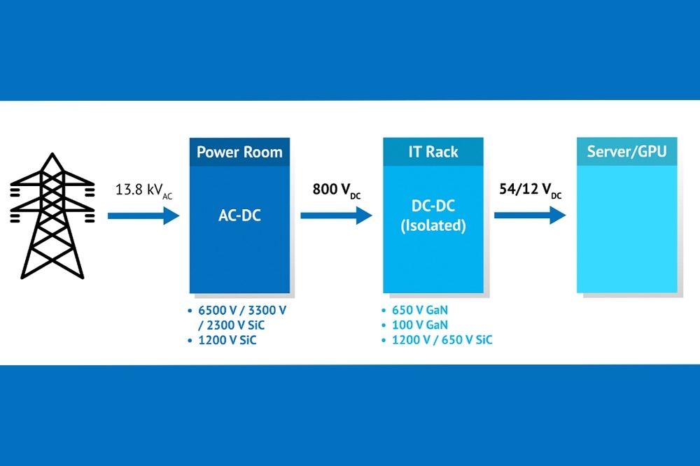
Now available in 200 mm and 300 mm, Power-SOI is a robust SOI technology that enables state-of-the-art gate drivers and power management ICs (PMICs). These Power-SOI based ICs simplify the design of SiC and GaN device platforms, improve reliability, and boost system performance in applications such as electric vehicles, industrial automation, renewable energy systems, and data center power supplies.
The following sections delve into the design considerations, operating principles, and performance benefits of Power-SOI technology, underscoring its pivotal role in the widespread adoption of next-generation WBG devices across various industries.
Figure 2. Vth Drift Over Time As Measured by GD3162 (Courtesy to NXP Semiconductors)
Gate Driver and PMIC’s trends and challenges
The adoption of WBG semiconductors in power conversion and motor control drives critical advancements in gate driver and power management IC (PMIC) technology. Evolving trends and challenges are now guiding the development of next-generation PMIC solutions, particularly on 300 mm wafers.
Higher Switching Frequency: WBG devices are switching at significantly higher frequencies compared to silicon-based devices, enabling higher power densities and improved system efficiency.
This performance represents challenges for gate driver ICs with:
• Managing higher dV/dt and dI/dt transients during switching transitions caused by parasitics in the circuit
• Minimizing propagation delays and ensuring precise timing control
• Providing adequate and well controlled drive strength to charge and discharge gate capacitances quickly as the gate drive strength of WBG devices is significantly lower than silicon devices
Figure 3. Typical half bridge (HB) topology [1]
Higher Voltages and Operating Temperatures: WBG devices operate at higher voltages (> 1200V) with higher junction temperatures (Tj) (> 175°C) compared to silicon. Gate driver ICs must withstand these extreme conditions while ensuring reliable operation, requiring:
• High voltage isolation and robust circuit protection
• Stable operation across a wide temperature range
• Careful layout and packaging considerations for harsh environments
Much More Dense Integration Of Intelligent Features: To simplify system design and improve reliability, gate driver ICs are evolving towards higher integration of intelligent features:
• Integrated power stages and low-side/high-side drivers
• Advanced monitoring and protection (desaturation, overcurrent, undervoltage lockout) with increasing digital blocks (e.g. non-volatile memory (NVM) etc.)
• Adaptive driving techniques (active Miller clamping, di/dt control etc.) and programmability
Figure 4. Basic silicon-on-insulator (SOI) as compared to bulk CMOS structure [2]
Automotive and Industrial Qualification:
As WBG devices find applications in automotive and industrial sectors, gate driver ICs must meet stringent quality and reliability standards :
• Automotive qualifications (AEC-Q100, ISO 26262) and industrial qualification (IEC61508)
• Robust electromagnetic compatibility (EMC) and electromagnetic interference (EMI) performance
• High manufacturing quality and traceability
Innovative gate driver solutions specifically designed for wide-bandgap power devices are crucial for realizing high-efficiency, high-density power conversion and motor control systems. The functionally safe NXP GD3162, for example, offers dynamic gate strength control, power device aging detection, and integrated fast (<1 µs) short-circuit detection, thereby improving efficiency and enhancing system safety.
With adjustable dynamic gate strength, the GD3162 optimizes gate current based on load requirements, reducing switching losses. Figure 1 shows efficiency gain test results using NXP’s power inverter reference design.
During a SiC power device’s lifetime, its threshold voltage (Vth) may shift, serving as a key reliability indicator. By tracking these shifts, the GD3162 supports power switch diagnostics and predictive reliability. Figure 2 shows the Vth drift over time as measured by the GD3162.
Figure 5. Example of NTSOA of an Auto Power-SOI based gate driver IC [2]
Power-SOI Technology: A Game-Changer in 300mm
Power-SOI is a key enabling technology that addresses evolving gate driver IC requirements and challenges for advanced WBG-based power devices.
Power-SOI is a key technology for high-speed switching
Power-SOI provides superior negative transient voltage robustness. In contrast, standard bulk-based integrated circuits tolerate only limited negative voltages – typically around –1 V – before generating uncontrolled substrate currents that disrupt gate driver IC operation. Because bulk-based gate driver circuits lack isolation, fast switching and circuit parasitics can induce oscillations and voltage swings, exposing IC pins to negative voltages. Figure 3 illustrates an example of negative voltage during gate driver operation.
When IGBT T1 is off, the motor’s inductive load generates a negative voltage at T2’s collector as the freewheeling current (Ifreewheeling) flows through T2’s freewheeling diode. Circuit parasitics (Cp and Lp) can exacerbate this effect, causing the half-bridge output voltage (VL) to swing to -20 V to -100 V for short durations.
Because VL is tied to the gate driver IC’s VS pin, these transients can disrupt operation or even damage the device. Hence, it is critical to ensure the gate driver IC pins can withstand such
negative voltages and incorporate robust internal protection.
Power-SOI, developed using Soitec’s Smart Cut™ process, is an advanced SOI technology, widely adopted by smart gate driver ICs. Its buried oxide (BOX) layer isolates the active region from the silicon substrate, significantly reducing parasitic capacitance and preventing leakage or latch-up between adjacent devices. Figure 4 compares Power-SOI and bulk CMOS substrates. By insulating the active area from the substrate, the BOX inherently improves immunity to negative voltages, enhancing the negative transient safe operating area (NTSOA) of gate driver ICs. Figure 5 shows an example of the NTSOA for a Power-SOI-based gate driver IC [2].
The superior NTSOA enabled by PowerSOI allows the gate driver IC to support higher switching frequencies with good performance and no unexpected disturbances.
Fig 6. Example of the comparison of Auto Power-SOI based gate driver IC and bulk based gate driver IC [2]
Power-SOI supports smaller PN junctions by leveraging its BOX layer to reduce parasitic capacitances. A lateral high-voltage, low on-resistance device can be implemented using double RESURF (reduced surface field) technology, combined with a simple local oxidation (LOCOS) process, the BOX layer, and thin drift regions in the top SOI film. This design lowers on-resistance per area and reduces gate capacitance, enabling gate driver ICs to achieve higher switching frequencies.
It also minimizes propagation delays, ensuring precise timing control and sufficient drive strength for rapid gate charging and discharging of external MOS devices.
Power-SOI further reduces power dissipation at high switching frequencies by lowering device gate capacitance, resulting in lower switching losses than comparable bulk-based gate driver ICs. As shown in Figure 6, this improvement enables higher operating frequencies and confirms Power-SOI’s superior efficiency and performance [2]
Power-SOI technology supports higher voltages and temperatures, enabling greater monolithic integration of high- and low-voltage blocks on the same die. By combining Power-SOI substrates with deep trench isolation (DTI), Power-SOI reduces the overall die footprint while providing robust dielectric isolation via its BOX layer. This isolation mitigates latch-up and parasitic coupling, while DTI structures form vertical barriers that allow high- and low-voltage devices to coexist in close proximity. Figure 7 compares the device-to-device isolation spacing among current technologies [3].
Power-SOI exhibits low leakage currents at high temperatures, making it well-suited for high-frequency power devices. Its BOX layer isolates the active region from the substrate, suppressing leakage paths that typically increase exponentially with temperature in bulk devices. Figure 8 compares leakage currents for both Power-SOI with DTI and bulk substrates with junction isolation [4].
Power-SOI’s exceptionally low leakage current above 125 °C simplifies high-precision analog circuit design by eliminating the need for extensive temperature compensation, enabling reference circuits with reduced voltage and gain drift. This improves gate driver performance and reliability in high-temperature applications.
Fig 7. Device-to-device isolation spacing based on BCD with Power-SOI
and DTI, BCD with bulk and DTI and BCD with bulk and junction isolation
[3]
Power-SOI enables greater integration of intelligent features
As highlighted in the previous session, Power-SOI technology enables monolithic integration of high- and low-voltage blocks on a single die, reducing the overall footprint. This allows incorporation of power stages, low- and high-side drivers, and advanced monitoring and protection features within a single smart gate driver IC. Meanwhile, its BOX and DTI structures minimize noise coupling and crosstalk, streamlining the integration of next-generation gate driver ICs with intelligent features.
Power-SOI enables monolithic integration of a bootstrap diode and resistor on the gate driver die, eliminating external components and reducing system costs as well as total cost of ownership (TCO). It also allows on-chip monitoring features, such as switch node voltage and high-side switch status, lowering both BOM and PCB area, particularly in three-phase motor drives. Furthermore, Power-SOI simplifies co-packaging of gate driver chips and WBG transistors, increasing integration, boosting power density, and placing protection circuits closer to the power switches.
Power-SOI is fully qualified for automotive and industrial applications
The demand for higher functional safety (FuSa) requirements such as automotive ISO26262 and industrial IEC61508 is getting higher with the rising of higher autonomous driving level and factory automations (e.g. industry 4.0 & 5.0, digital twins factory etc.).
Power-SOI eases the design of higher functional safety (Fusa) level ICs. Power-SOI enables higher monolithic integration, reducing the chip count per system. Fewer components decrease the overall system failure-in-time (FIT) rate by minimizing interconnect and other failure points. This chip-level integration enhances system reliability, a critical requirement for achieving automotive and industrial functional safety targets. The monolithic integration facilitated by Power-SOI’s DTI & BOX isolations directly improves the mean time between failures (MTBF) for safety-critical applications.
Fig 8. Comparison of leakage currents for Power-SOI with DTI and bulk substrate with junction isolation [4]
Power-SOI’s high robustness and high reliability ease the qualifications
Power-SOI enhances electromagnetic compatibility (EMC) and reduces electromagnetic interference (EMI) through symmetric output stages and device isolation. Its BOX layer ensures complete isolation and prevents substrate noise propagation, while DTI and BOX minimize crosstalk.
Power-SOI’s isolation enables high-voltage ESD protection by cascading low-voltage protection devices without introducing parasitic elements, optimizing the ESD-protection window in high-voltage designs. Additionally, replacing deep N-well junction isolation with DTI reduces the ESD layout area.
With intrinsic robustness against latch-up, ESD, EMC, and EMI, Power-SOI minimizes systematic faults from manufacturing. Its BOX and DTI layers enhance reliability, reducing the need for complex design techniques to manage process-induced faults. This simplifies the development of high-functional safety (FuSa) systems compliant with stringent automotive and industrial standards like ISO 26262 and IEC 61508.
With Power-SOI’s superior low leakage current at high junction temperature as explained in previous session., it is easy to develop next generation gate driver IC passing AEC-Q100C gate 0 requirements.
And now, Power-SOI is available in 300mm
Power-SOI has been produced by SOITEC for decades in 200mm and smaller wafer sizes, with typical SOI top layer thickness in the micrometer range. Leveraging its Smart Cut™ technology, SOITEC has delivered millions of
SOI wafers.
A transition from 200mm to 300mm is now underway among key Power-SOI players, driven by the need for better integration with advanced semiconductor manufacturing tools. To support this shift, SOITEC now offers thicker SOI wafers, combining Smart Cut™ technology with monocrystalline epitaxy. This process enables the growth of high-quality thick SOI layers with excellent crystallinity, precise control over resistivity and thickness uniformity, and minimal defectivity.
Conclusion
Power-SOI technology is a key enabler for advanced gate drivers and power management ICs, optimizing power conversion for WBG devices in fast-growing markets. Its monolithic integration, utilizing DTI and BOX layers, produces more compact, reliable ICs with inherent resistance to latch-up, ESD, and EMC/EMI issues, enhancing overall system reliability.
By reducing chip count, PowerSOI lowers system FIT rates and improves functional safety, meeting stringent automotive standards like ISO 26262 ASIL-D and IEC 61508 SIL-4. With 300mm availability, its adoption is expanding in EVs, renewable energy, and data center power systems.
PowerSOI continues to drive innovation, meeting the industry’s evolving demands for performance, safety and efficiency.


