Scientists make first gallium oxide pn diodes
Researchers at Nagoya University in Japan have created the first functional pn diodes using Ga2O3.
Their method 'P-type layer formation study for Ga2O3 by employing Ni ion implantation with two-step oxygen plasma and thermal annealing' was published in the Journal of Applied Physics.
SiC-based Schottky barrier diodes are replacing silicon devices in inverter applications. However, high production costs due to SiC substrates being deposited by PVD and high device processing temperatures are barriers to increasing their market scale. SiC also faces another difficulty in that it tends to degrade when used in bipolar pn junction devices.
Ga2O3 is a potential alternative because it is less expensive to produce than SiC as a result of its compatibility with melt-growth methods such as the film-fed growth or Czochralski method. Schottky barrier diodes based on Ga2O3 are under development; however, practical bipolar pn diodes have not yet been achieved.
The problem is that Ga2O3's crystal structure easily accepts the atoms needed to create n-type layers but rejects the atoms required for p-type layers. Previous methods to force them in either failed or required temperatures that destroyed the material. Without both types working together, Ga2O3 remained limited for practical applications.
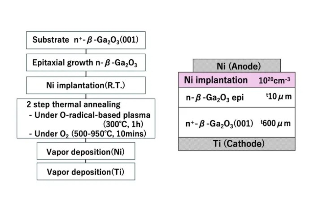
To address this, the researchers injected nickel atoms into the Ga2O3 layer by shooting individual atoms at high speed into the surface of the material. They then heated the material twice, first at 300°C with activated oxygen radicals (oxygen atoms that have been given extra energy using proprietary plasma treatment) and then at 950°C in oxygen gas. This converted the embedded nickel into nickel oxide and properly integrated it with the Ga2O3 crystal structure.
“Since this method uses standard industrial equipment and processes, it can be scaled up for mass production,” Masaru Hori from the Center for Low-Temperature Plasma Sciences at Nagoya University highlighted. “The implications for future energy efficiency and costs are substantial, particularly for electric vehicle and renewable energy industries.”
Nagoya University spin-off company NU-Rei is now working to bring these advances to market.
Pictured above: Illustration of the new fabrication process: ion implantation of nickel atoms, followed by low-temperature plasma treatment and high-temperature annealing (heating) to create stable p-type layers in Ga2O3 .
Reference
Naohiro Shimizu et al; J. Appl. Phys. 14 August 2025; 138 (6)