NCT achieves record Ga₂O₃ performance
Novel Crystal Technology (NCT), has announced the successful development of a Gallium Oxide vertical MOS transistor (β-Ga2O3 MOSFET) with 1.23 GW/cm2 Power Figure of Merit (PFOM).
This PFOM is believed to be the world's highest value for β-Ga2O3 FETs and is 3.2 times higher than the previous highest value published by other research institutes.
Part of this R&D effort was subsidised under the 'Research and Development of Inversion-type channel Gallium Oxide MOS Transistors' program of the National Security Technology Research Promotion Fund (JP004596) of the Acquisition, Technology and Logistics Agency (ATLA) in Japan.
According to NCT, The results will greatly advance the development of medium- to high- voltage (0.6—10 kV) Ga2O3 transistors, which will lead to lower prices and higher performance of power electronics.
Details of these results was presented at the 72nd JSAP Spring Meeting on March 15, 2025, 'Demonstration of β-Ga2O3 FinFET with power figure of merit of 1.23 GW/cm2'.
WBG materials SiC and GaN are replacing silicon power devices in many applications but β-Ga2O3 has even better material properties, and cost is more competitive due to faster crystal growth speed. It is expected to be applied to various power electronic devices such as home appliances, industrial equipment, electric vehicles, trains, solar power generation, and wind power generation, because of its low-loss and low-cost characteristics.
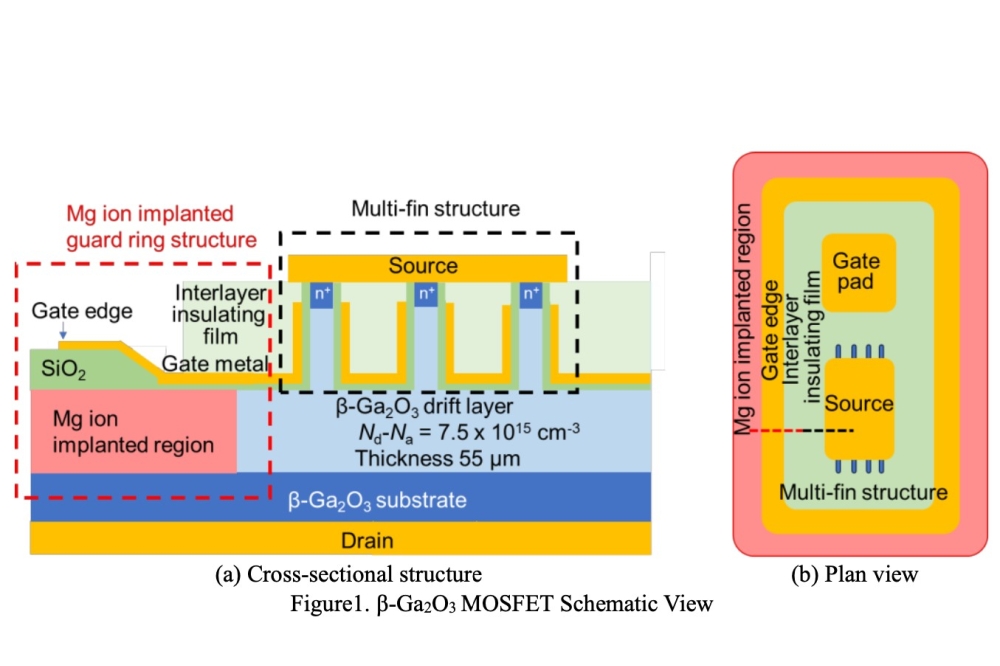
NCT has been working on commercialisation of β-Ga2O3 MOSFETs since 2019. This time, the world’s highest PFOM for β-Ga2O3 MOSFETs, 1.23 GW/cm2 was achieved by incorporating a high-resistance guard ring structure with Mg ion implantation at the edge of gate electrode in a drift layer.
Although NCT has been developing β-Ga2O3 MOSFETs for a while, the material’s superior high breakdown electric field strength (6—8 MV/cm) has not been fully exploited, due to the high electric field at the edge of the gate electrode.
In other materials, a p-type conductive layer is used at the edge of the electrode to reduce the electric field, but for Ga2O3, the p-type conductive layer technology has not yet been established, and the same method could not be applied.
So instead of the technically unestablished p-type conductive layer, NCT’s researchers used a high-resistance β-Ga2O3 layer for the guard ring, and Mg, an acceptor impurity that forms a deep level, was added to the layer through ion implantation and activation heat treatment processes.
The prototype β-Ga2O3 MOSFET has 10 fins with a mesa width of 0.2 μm, a gate length of 3.5 μm, a fin length of 70 μm, and a fin pitch of 5 μm.
Figure 1 (above) shows the cross-sectional structure and plan view of the newly developed β-Ga2O3 MOSFET. The features of the transistor are as follows.
・Vertical device structure that is advantageous for low loss and high current required for power devices
・Multi-fin structure with sub-micron mesa width channel that enable normally-off operation without a p-type conductive layer
・β-Ga2O3 drift layer with a low donor concentration of 7.5×1015 cm-3, and a thick thickness of 55 μm.
・Guard-ring structure with Mg ion implantation to β-Ga2O3in the area around the gate edge to reduce the electric field at the region.
For the future, NCT says the termination structure of β-Ga2O3 MOSFETs can be enhanced by using hetero p-type semiconductor materials such as NiO, etc., to further reduce the electric field concentration at the electrode termination.
The researchers aim to realise a β-Ga2O3power transistor with performance exceeding that of SiC’s by exploiting the potential of β-Ga2O3 high breakdown field strength (6—8 MV/cm) with an advanced termination structure.