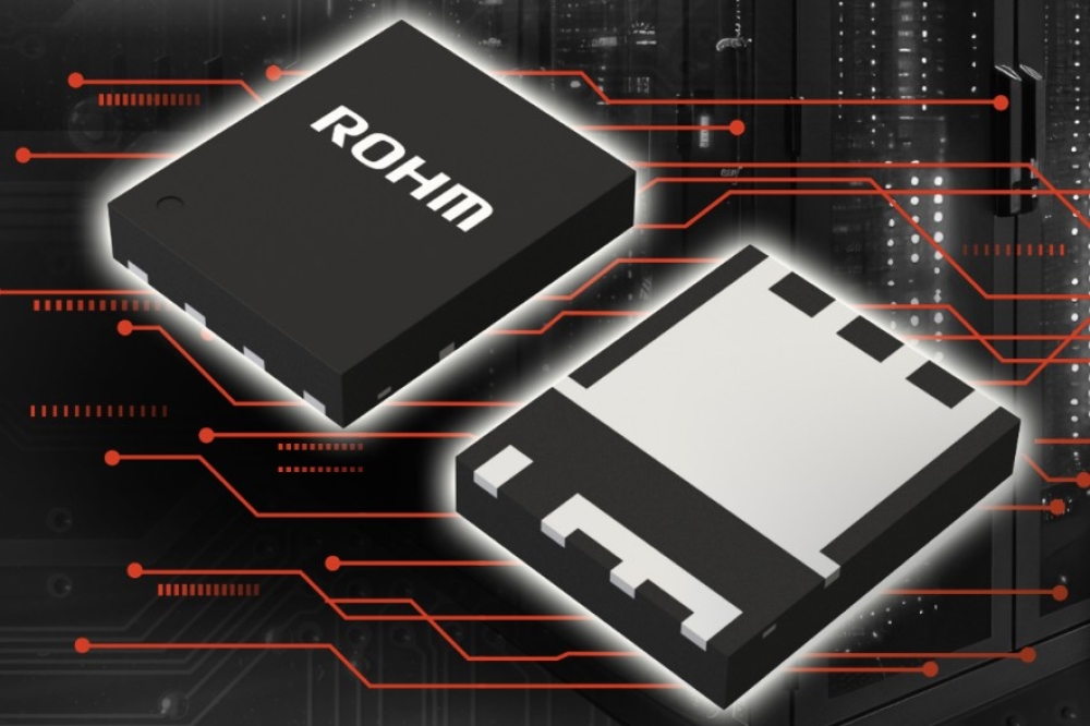
Infineon GaN family has integrated Schottky diode
Infineon Technologies has introduced the world’s first GaN power transistors with integrated Schottky diode for industrial use.
Accordany to the company, the family of medium-voltage CoolGaN Transistors G5 with integrated Schottky diode increases the performance of power systems by reducing undesired dead-time losses, thereby further increasing overall system efficiency. Additionally, the integrated solution simplifies the power stage design and reduces BOM cost.
In hard-switching applications, GaN-based topologies may incur higher power losses due to the larger effective body diode voltage (V SD) of GaN devices. This gets worse with long controller dead-times, resulting in lower efficiency than targeted.
Until now, power design engineers often require an external Schottky diode in parallel with the GaN transistor or try to reduce dead-times via their controllers. All of which is extra effort, time and cost. The new CoolGaN Transistor G5 from Infineon reduces these challenges in applications including server and telecom IBCs, DC-DC converters, synchronous rectifiers for USB-C battery chargers, high-power PSUs, and motor drives.
GaN transistor reverse conduction voltage (V RC) is dependent on the threshold voltage (V TH) and the OFF-state gate bias (V GS) due to the lack of body diode. Moreover, the V TH of a GaN transistor is typically higher than the turn-on voltage of a silicon diode leading to a disadvantage during the reverse conduction operation, also known as third quadrant. Hence, with this new CoolGaN Transistor, reverse conduction losses are lower, compatibility with a wider range of high-side gate drivers, and with deadtime relaxed, there is broader controller compatibility resulting in simpler design.
The first of several GaN transistors with integrated Schottky diode is the 100 V 1.5 mΩ transistor in 3 x 5 mm PQFN package.