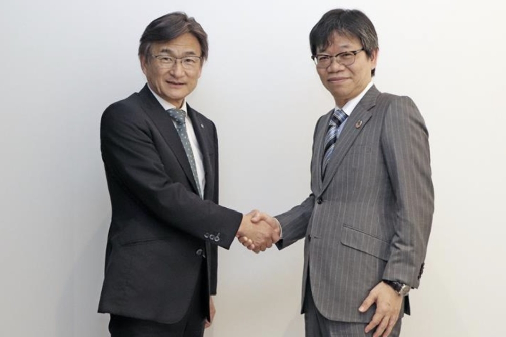
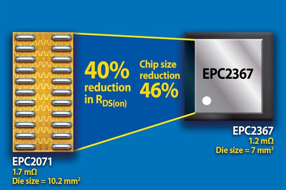
ST and Innoscience sign GaN deal

STMicroelectronics and Innoscience have signed an agreement on GaN technology development and manufacturing.
The joint development initiative allows Innoscience to use ST’s front-end manufacturing capacity outside China for its GaN wafers, while ST can use Innoscience’s front-end manufacturing capacity in China for its own GaN wafers.
The common ambition is for each company to expand their individual offering in GaN with supply chain flexibility and resilience to cover all customers’ requirements in a wide range of applications.
Marco Cassis, president, analogue, power and discrete, MEMS and sensors of STMicroelectronics said: With this agreement we will leverage this model to the benefit of our customers globally. First, ST will be accelerating its roadmap in GaN power technology to complement its silicon and SiC offering. Second, ST will be able to leverage a flexible manufacturing model to serve customers globally.”
Weiwei Luo, chairman and founder of Innoscience, said:“GaN technology is essential to improve electronics, creating smaller and more efficient systems which save electric power, lower cost, and reduce CO2 Emissions."
He added: "The joint collaboration between ST and Innoscience will further expand and accelerate the adoption of GaN technology. Together the teams at Innoscience and ST will develop the next generations of GaN technology”.