NREL team advances substrate engineering
Researchers from the National Renewable Energy Laboratory (NREL), the Colorado School of Mines, and Oak Ridge National Laboratory have examined a potential route to achieve peak performance of AlxGa1–xN, a key material for increasing power electronics' energy efficiency and performance, through growth on optimised substrate materials.
This work was undertaken with funding support from the microelectronics initiative through the US Department of Energy Basic Energy Sciences Office and Advanced Scientific Computing Research program.
The goal is to grow higher-quality materials through the selection of a lattice-matched substrate. Better electron transmission means better device performance, but the growth of AlxGa1–xN on lattice-mismatched substrates leads to dislocation (line defects that distort a lattice due to the misalignment of atoms), resulting in diminished performance.
"Substrate engineering enables the use of high-performing materials in real devices," said NREL's Dennice Roberts, a materials science researcher. "If we can engineer lattice-matched substrates to reduce the effect of dislocations, we can widen the range of sufficiently high-quality materials and build better, more energy-efficient power electronics."
As detailed in a new paper, 'Designing TaC Virtual Substrates for Vertical AlxGa1–xN Power Electronics Devices', published in PRX Energy, the research team proposed and demonstrated that electrically conductive, lattice-matched tantalum carbide (TaC) can act as a suitable substrate for AlxGa1–xN epitaxy that may meet growing power needs.
Benefits of transition metal carbides for AlxGa1–xN growth
Defects, such as substrate cracking, are common with growth on AlN and GaN. Efforts to reduce dislocation have been effective but often increase device complexity and limit device design and performance. Lattice mismatching, again, leads to device performance issues.
"Lattice matching is critical for high-quality epitaxial growth," Roberts said. "We hypothesised that substrates from transition metal carbide and nitride families could enable desired conditions for AlxGa1–xN growth, not only because of ideal lattice matching but also because of ideal thermal and electrical conductivity properties. TaC and AlxGa1–xN are closely lattice-matched, TaC is highly conductive, and they display matched growth in size in response to changes in temperature."
The team grew, prepared, and used TaC thin films as virtual substrates for high-aluminum-content AlxGa1–xN and demonstrated AlxGa1–xN growth on TaC virtual substrates. To precisely and effectively deposit TaC onto the substrate, they used radio frequency sputtering. They formed substrates through high-temperature annealing, a process that increases ductility—the ability of a metal to undergo significant stress before cracking or breaking—and reduces defects.
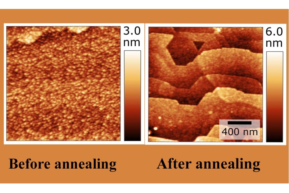
Atomic force microscopy (AFM) shows the surface of the TaC thin film before and after annealing at high temperatures (see pic above). The initial film surface is composed of many columnar grains, whereas after annealing the surface has reoriented to plateaus or "step terraces." This flatter surface facilitates growth of much higher quality AlGaN layers and thus leads to higher performing electronics.
Motivated by the work of Roberts and her coauthors, NREL materials science postdoctoral researcher Sharad Mahatara and NREL senior scientist Stephan Lany approached the problem of interfaces between materials with different crystal structures from a computational perspective.
Their work, 'Heterostructural Interface Engineering for Ultrawide-Gap Nitrides From First Principles: TaC/AlN and TaC/GaN Rocksalt-Wurtzite Interfaces,' was recently published in Physical Review Applied. The broader context of this study is that lattice-matched substrates with the same crystal structure are often unavailable. Therefore, there are new opportunities to use heterostructural interfaces for conversion and control, if the formation of these more complex interfaces can be understood and controlled.
The formation of interfaces between rocksalt structure (rs) and wurtzite structure (wz) materials—e.g., between TaC and AlN (GaN) films—can be modeled by considering the different possibilities of stacking the individual atomic layers. This problem is somewhat related to the question of how to arrange oranges in a box so as to get as many as possible into it.
The NREL researchers approached this problem by writing a computer code with an algorithm to systematically enumerate the possible stacking sequences within a few atomic layers near the interface. This algorithm can be used to understand the atomic structures of various commensurate rs/wz interfaces, including the oxide interfaces.
Mahatara and Lany then used first-principles density functional theory calculations to determine the most energetically stable atomic structure arrangement for each combination of substrate termination (the type of the last substrate atomic layer, Ta or C), film nucleation (the first nitride film layer, Al/Ga or N), and wz polarity (Al/Ga or N polarity, describing the orientation of the atomic bonds). Additionally, they used this data to predict which of the combinations will be most favorable under different experimental synthesis conditions.
This information is important because the detailed atomic structure at the interface will determine the material's functionality and performance in a device.
For example, the polarity affects electric fields that are responsible for the transport of electrons across the interface. Controlling the polarity of the film during growth is therefore an important aspect of AlGaN epitaxy.
"Our results may guide experimentalists on how to regulate nitrogen-polarity against metal-polarity of nitride films grown on TaC substrates as a function of growth conditions," Mahatara said.
As a follow-on to the current work, Mahatara and Lany are now investigating the electronic properties of their predicted structures. This ongoing effort will provide further information and predictions on how these structures will act and perform in new device concepts. The goal is to give experimentalists critical data for rational device design to accelerate the development of novel concepts in microelectronics.
The findings from both studies may inform substrate engineering that improves power electronics as the needs of an electrified future grow.
"We're excited about the potential for these materials to address power and energy efficiency challenges," Roberts said. "From a research perspective, it's really neat to see a creative solution to a longstanding problem look like it has a lot of promise in real world applications, so we look forward to the developments to come."