4-inch gallium oxide facility established in Swansea
Researchers at the Centre for Integrated Semiconductor Materials (CISM) at Swansea University have established the first 4-inch thin film gallium oxide (Ga₂O₃) capability in the UK.
This advance was achieved using a newly commissioned Aixtron close-coupled showerhead deposition system, that can precisely grow high-quality crystalline thin film gallium oxide on 4-inch substrates. These have been tested and shown to be uniform and of high quality.
This capability is housed in the new Oxide and Chalcogenide MOCVD Laboratory at CISM, which is now set to become a national hub for thin film gallium oxide research and development in areas such as power electronics, deep-UV photodetectors and transparent conductive oxide applications.
Dan Lamb, research lead at the Oxide and Chalcogenide MOCVD Centre said: “This new facility represents a major step forward for our research, and I’m incredibly excited about the possibilities it unlocks for novel materials and device development. With this advanced equipment, we can push the boundaries of our existing work while also creating new opportunities for collaboration with research groups across the UK and beyond."
John Heffernan of the National Epitaxy Facility, which supports semiconductor research in UK universities, said:“Swansea University’s MOCVD capability is now accessible to researchers through direct collaboration. Researchers can also gain access to feasibility studies through Swansea partnering with the UK National Epitaxy Facility’s Pump Priming scheme. This initiative ensures that academic and industrial partners can leverage Swansea’s expertise in epitaxial thin film growth to accelerate their research and technology development.’
Sam Evans, director of quality assurance and external affairs, Vishay Newport, said:"This is a major step forward for wide band gap materials innovation in our South Wales Semiconductor Cluster, underpinning efforts to grow regional manufacturing in advanced power electronics such as Vishay’s recently announced £250M investment in SiC component expansion.”
The deposition system was funded by a £2.7m grant from the Engineering and Physical Sciences Research Council (EPSRC – Strategic Equipment Programme), reinforcing the UK’s commitment to advancing semiconductor innovation.
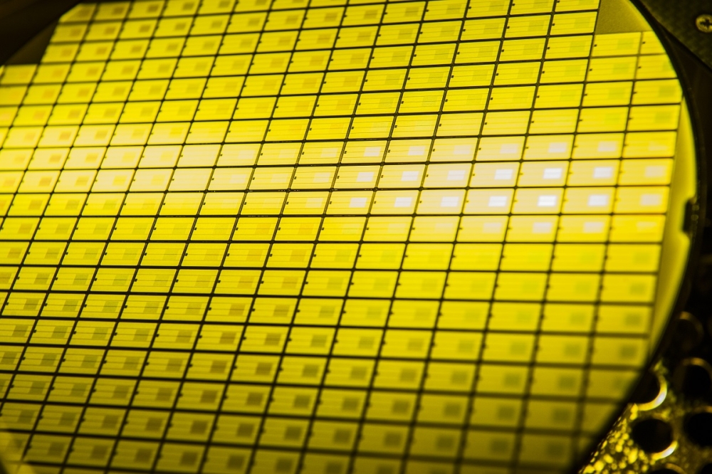
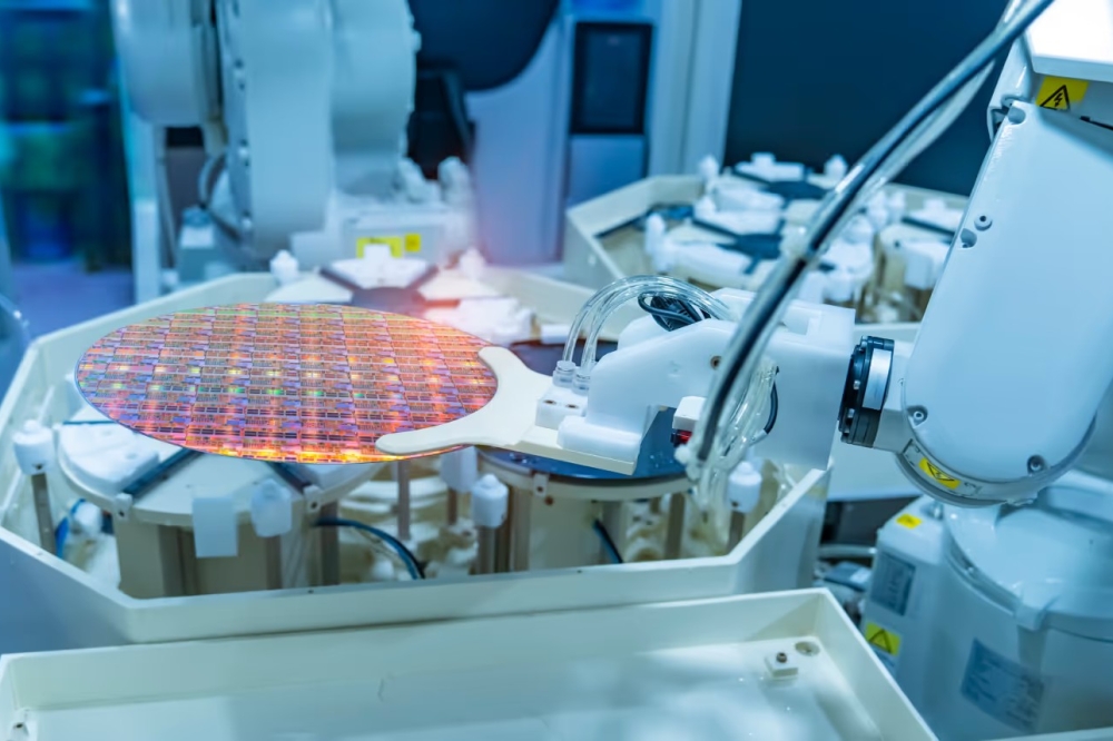
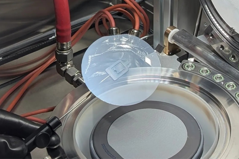
Pictured above: The Aixtron close-coupled showerhead at the Oxide and Chalcogenide MOCVD reactor with 4-inch gallium oxide thin film on sapphire wafer being unloaded.