Keysight unveils 3kV wafer test system for power semis
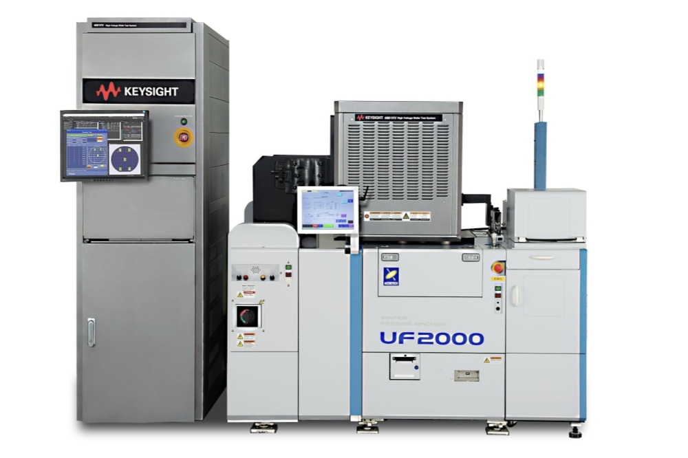
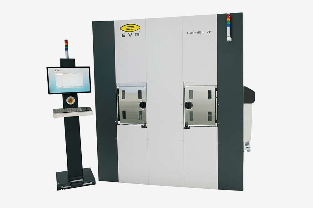
Keysight Technologies has introduced a 4881HV High Voltage Wafer Test System designed to improve the productivity of power semiconductor manufacturers by enabling parametric tests up to 3kV supporting high and low-voltage in one-pass test.
Manufacturers have traditionally measured wafers using separate testers for high and low voltages. However, demand for power semiconductors is rapidly growing due to their multifunctionality, higher performance, and next-generation devices such as SiC and GaN. As a result, customers need a solution to more accurately and efficiently test their devices and reduce time to market.
Keysight’s solution addresses these challenges by allowing power device makers to perform process control monitoring (PCM) and wafer acceptance testing (WAT) in manufacturing.
The new test system's high-voltage switching matrix (HV-SWM) is scalable up to 29 pins, and integrates with precision source measure units (SMUs). It enables highly flexible measurements from low current down to sub-pA resolution up to 3kV at any pins. Additionally, high-voltage capacitance measurement and various parametric tests are supported.
The test system has built-in protection circuitry and machine control, ensuring operators and equipment are not impacted by high-voltage surges during a test, and is compliant with safety regulations, including SEMI S2 standards.


