Atomera/Sandia project to address GaN/Si challenges
Atomera, a US semiconductor materials and technology licensing company, has announced a project at Sandia National Laboratories (a US Department of Energy, research centre), to address the challenges of growing GaN films on silicon.
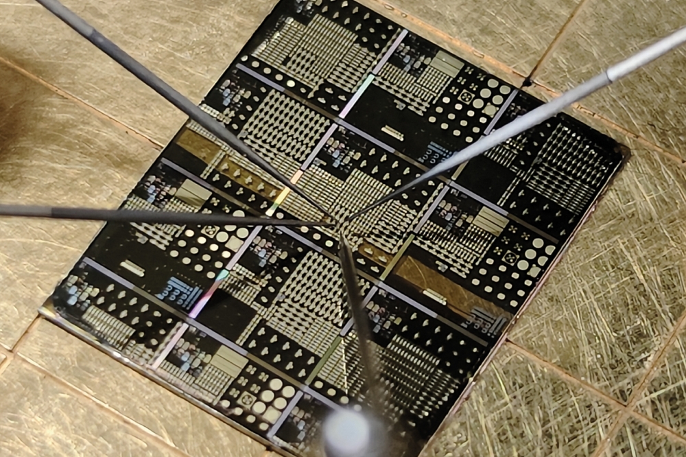
The project, which is a collaboration with the Centre for Integrated Nanotechnologies (CINT) at Sandia, aims to create the world’s first GaN transistors and test data from wafers employing Atomera’s Mears Silicon Technology (MST). The effort will build upon improvements already observed at the materials level in GaN/MST on silicon wafers.
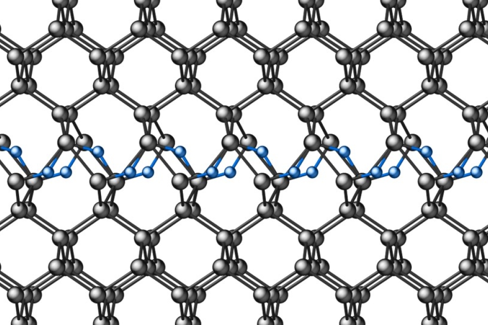
MST consists of layers of a non-semiconductor, such as oxygen inserted into a semiconductor material, such as silicon so that epitaxial growth is preserved. These layers can be used to modify or enhance the basic semiconductor properties and device attributes in a number of ways, including: diffusion blocking, variability, mobility, gate leakage, and reliability, among others.
“Atomera’s MST represents a tremendous opportunity to improve GaN on Si manufacturing and provide speed, efficiency and cost-saving benefits to a wide range of industries including electronics, RF/microwave electronics and even MicroLEDs. This user project will test the effectiveness of the MST solution quickly using CINT’s highly specialized tools and technology and give Atomera access to our team of scientists and researchers,” said Jeffrey Nelson, director of CINT.
Due to the limited availability and size of native substrates, most GaN devices have been grown heteroepitaxially on sapphire, SiC or Si substrates. Although impressive performance has been achieved with each of these, Si substrates offer a clear pathway to large wafer size, low cost and compatibility with well-established CMOS wafer fabrication lines.
However, there are significant challenges, including wafer warping or cracking, associated with the growth of thick GaN films on Si (GaN/Si), particularly at large wafer sizes.
“Over the past approximately 25 years, GaN has transformed multiple industries, including lighting, RF/microwave and power electronics, but manufacturing limitations have hindered the widespread adoption of GaN for modern power electronics,” said Shawn Thomas, vice president of Marketing & Business Development at Atomera. “This user project with Sandia Labs will allow Atomera to fabricate devices and collect data to validate the mechanical and electrical benefits of MST-enhanced GaN on Si.”
Managing stress is the most important aspect of growing thick GaN epi on Si. Commercially available GaN on Si power electronics (PE) devices are currently limited to a ~650V rating due to the maximum epi thickness (and thus breakdown voltage) that can be grown on Si without excessive wafer curvature, micro-cracking or poor yield. MST can improve the growth of GaN epitaxy on Si substrates by relieving biaxial tensile stress.