High-voltage SiC for storage & MV-grid conversion
As reliance on renewable energy generation continues to increase, a
three-level converter architecture built using high-voltage SiC MOSFETs
enhanced with an integrated MPS diode boosts efficiency and reliability
in the
storage-to-grid connection.
By Ranbir Singh, EVP
GeneSiC, Navitas Semiconductor and Llew Vaughan-Edmunds, Senior Director
Product Management and Corporate Marketing, Navitas Semiconductor
Balancing the flow of energy into and out of the grid is a perennial challenge for operators, now made tougher as an increasing proportion of energy must come from renewable sources. Historically, pumped hydro-electric has dominated, representing more than 82% of grid-connected storage capacity. It is well suited to providing a long-lasting boost at times when high demand is expected, such as in the early evening.
Wind and solar, which are intermittent and unpredictable, demand storage with different characteristics including faster response time, low/medium energy capacity, easy scalability, and compact size. Battery energy-storage systems (BESS), typically built with Li-ion batteries, can meet these demands. BESS currently represents almost 17% of storage in the US, with about 16 GW of installed capacity in 2023.
Another 15 GW is planned for 2024. In addition to helping balance energy flow, BESS can also help improve the performance of the transmission and distribution network by compensating for disturbances such as voltage fluctuations, frequency variations, phase shifts, harmonics, and interruptions.
BESS to grid connection
The power-conversion network that connects the BESS to the medium-voltage (MV) grid at the utility premises must convert from DC at the battery voltage to AC at the grid voltage and frequency. The network also needs to provide isolation and must support bidirectional power flow to permit charging and discharging as the levels of power demand and generation fluctuate.
There is no standardized topology for the BESS-grid connection. A common approach is to combine a DC/DC converter at the battery with a two-level DC/AC stage, which may be a voltage-source converter for simplicity. Alternatively, this DC/AC stage can be an impedance-source converter (ZSC) to provide buck-boost flexibility. A low-pass filter removes injected harmonics and a transformer provides isolation as well as converting between the battery voltage and the grid voltage.
An alternative approach combines a dual active bridge (DAB) with an active front-end converter (AFEC), as in figure 1. The three-level, neutral-point clamped architecture allows simplified filtering, compared to the two-level topology. In addition, this arrangement reduces voltage stress across the MOSFETs, which helps enhance reliability.
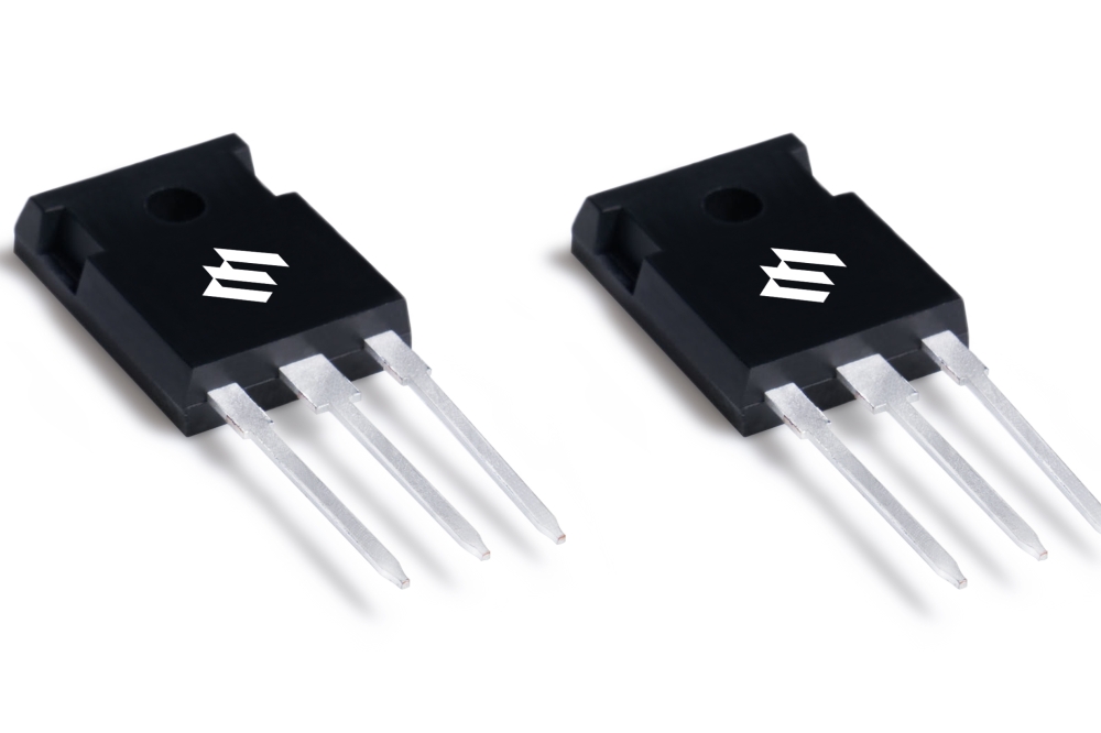
In the pursuit of maximum efficiency, silicon carbide power semiconductors have become the technology of choice in the converters used to connect the BESS to the MV grid. At the connection to the battery storage system, the DAB can be built with 1,200 V SiC MOSFETs. On the other hand, the MV-grid voltage can be as high as 13.8 kV or more. A suitable AFEC can be built using an array of silicon IGBTs or 1.7 kV SiC MOSFETs to safely handle the full MV-grid voltage. A different approach using 3.3 kV SiC MOSFETs allows a significant reduction in the component count, permitting smaller physical size, higher system efficiency, and lower operating temperature.
Enhanced SiC MOSFET structure In high-voltage, high-power applications like the three-level AFEC, a Schottky diode can be connected across each MOSFET to handle freewheel currents efficiently and improve reliability. A proportion of the current also passes through the MOSFET’s intrinsic body diode.
Conventional SiC MOSFETs can be vulnerable to faults at high applied voltage when the body diode is conducting. This is due to potential basal plane dislocations (BPD), which are defects present in the crystal structure from the earliest stages of SiC boule fabrication and wafer epitaxy. To overcome this, Navitas monolithically integrated a merged PiN-Schottky (MPS) diode with the 3.3 kV SiC MOSFET. In principle, MPS diodes combine the strengths of standard PN-junction (PiN) diodes, namely their high surge-current robustness and low reverse leakage, with the low forward voltage (VF) of a Schottky diode. The Schottky structure carries almost the entire current in normal operation, while the PiN diode conducts during high-current surges, which reduces dissipation and relieves thermal stress on the device.
Monolithic integration of the MPS structure in the 3.3 kV SiC MOSFET (figure 2) bypasses the built-in P-well/N-drift body-diode and so avoids the possibility of BPD faulting within the MOSFET N- drift layer. The inherently low VF of the MPS diode also effectively reduces the conduction and switching losses of the intrinsic body diode. Moreover, eliminating an externally packaged Schottky diode removes parasitic inductances associated with the physical connection and reduces the bill of materials. The integrated MPS diode also permits temperature-independent switching and simplifies device paralleling.
Testing the 3.3 kV SiC/MPS devices
Unclamped inductive switching (UIS) measurements have been performed to investigate avalanche robustness of the 3.3 kV SiC devices for AFEC applications. Inspecting the drain current/voltage waveforms at 30A peak drain current, as seen in figure 3, shows that the drain voltage peaks at 4,200 V during the test.
The maximum avalanche-withstand time (tAV) is 35 μs and single-pulse avalanche energy (EAS) is 2.6 Joules. In comparison, the test performed on a discrete 3.3 kV discrete SiC MOSFET with the same load-inductance showed an EAS of 4.8 Joules.
Short-circuit robustness of the GeneSiC MOSFETs was evaluated by connecting 3.3 kV discrete SiC MOSFETs, mounted on a 25°C baseplate, to a 1,200 V DC link. Devices both with and without monolithically integrated MPS diodes were tested. The devices were operated with +20 V / -5 V gate-drive. The drain current increases to a maximum of 525 A during the short-circuit pulse, as figure 4 shows. The short-circuit withstand time was measured to be 4.5μs.
Hybrid architecture – ‘Trench Assisted Planar’ technology
SiC MOSFETs are typically fabricated using either planar or trench architecture. Planar fabrication allows high process yield, while its relatively simple device structure enables excellent reliability. On the other hand, trench devices typically have higher RDS(ON) per die area and a figure of merit (FOM) that allows for faster switching performance.
Navitas’ trench-assisted planar’ technology architecture combines the higher yield and reliability advantages of the planar structure with the low RDS(ON) per die area, fast switching, associated with trench technology. Building 3.3 kV MOSFETs that combine this hybrid architecture with the integrated MPS diode creates a power switch that is well suited to use in three-level AFECs at the MV-grid voltage in BESS applications.
Conclusion
Battery storage has the characteristics needed to balance supply and demand in utility grids that are becoming increasingly reliant on renewable energy sources. The battery array needs an efficient, robust, and reliable connection to the medium-voltage grid. This circuit must convert between the battery and MV-grid voltages as well as allowing bidirectional operation for charging and discharging of the battery. Silicon carbide is the power technology of choice, for its switching efficiency and its ability to withstand high applied voltage, short-circuit current, and avalanche energy.
A three-level front-end converter built with 3.3 kV SiC MOSFETs ensures high efficiency and requires minimal filtering. With the added benefit of an integrated MPS diode, these devices deliver enhanced reliability while also handling freewheeling currents efficiently and minimising component count and parasitic circuit inductances.


