Cost-effective SiC substrate manufacturing for power devices enabled by oxide-free wafer bonding
Silicon Carbide (SiC) power devices are seen as a game-changer in the automotive industry.
By Bernd Dielacher and Peter Kerepesi, EV Group
These advanced semiconductor devices offer superior device performance compared to conventional silicon-based devices. SiC as a material has a 3x wider bandgap, 10x higher breakdown voltage and a 5x higher thermal conductivity.
These properties ultimately translate into faster EV charging and more efficient and reliable automotive fleets. Large investments in new SiC wafer fabs underline the high interest from the automotive sector. However, SiC manufacturing processes are far from being as mature as silicon processes. Significant developments along the entire process chain are needed to pave the way for a SiC-based future of the EV industry.

Figure 1. SiC power MOSFET structure using a cost-effective
engineered substrate (thin high quality monocrystalline SiC layer bonded
on a less-expensive SiC substrate)
Challenges include the high costs associated with substrate manufacturing, the complex processing of SiC, limited economies of scale and overall yield issues. In particular, the substrate is a major concern as it accounts for the largest share of production costs. Many routes are currently being explored to address this issue including improvements of crystal growth or novel wafer slicing technologies. The transition to 8-inch manufacturing is also expected to reduce substrate costs. This will only pay off in the long term as the processes for this scale are more complex and still need to be established and optimized. Another way of reducing substrate costs is the use of wafer bonding to utilize the expensive high quality SiC material more efficiently.

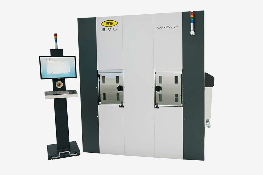
Figure 2. EVG ComBond® - Automated High-Vacuum Wafer Bonding System
Wafer bonding is an established process in power device manufacturing, in particular temporary bonding is commonly used to support substrates during device thinning. Wafer bonding is not only used for device manufacturing, but also enables new types of substrates. In the case of SiC MOSFET power devices, the main structure is built into a thin epitaxial SiC layer, commonly grown on monocrystalline SiC wafers. SiC crystal growth defects can be minimized or eliminated during the epitaxial process and epi-layers can be efficiently electrically tuned by doping.
However, only high-quality monocrystalline SiC substrates provide the required electrical device performance but contribute significantly to the overall chip cost. Since this material is mainly required as a seed layer for the epitaxial process, using only a thin layer and substituting the bulk material with a polycrystalline or lower quality monocrystalline substrate is seen as a viable route to address this cost issue (Figure 1).
Such a process generally involves wafer bonding of the two materials as well as a method to produce a thin layer from the high-quality monocrystalline substrate and reuse the remaining substrate multiple times. Several methods for the thin layer generation have been demonstrated, including the well-known ion-implantation and splitting process. This article focuses on the wafer bonding process and presents the latest developments for this application using EVGs high-vacuum ComBond® cluster system.

Figure 3. Oxide-free wafer bonding process of SiC using EVG ComBond® technology
The ComBond® system (Figure 2) offers covalent fusion bonding at room temperature, enabling heterogenous integration of various materials with different lattice constants and thermal expansion coefficients. Processing at room temperature does not induce additional stress in the materials, thus initial wafer bow is not increased. While classical fusion bonding is based on oxide-oxide bonding, the ComBond® process relies on a surface activation process called ComBond Activation, which is based on oxide removal by ion beam sputtering. Any re-oxidation is prevented by wafer handling and bonding the wafers in an ultrahigh vacuum environment. The result is a seamless transition between the two bulk materials without any intermediate layer. Table 1 summarizes the key differences between the two technologies. Oxide-free wafer bonding enables electrically conductive interfaces, which is the most important requirement for engineered substrates with respect to the structure of vertical SiC power MOSFETs.

Figure 4. Bonding energy optimization with respect to surface activation.
Oxide-free SiC-SiC wafer bonding optimisation and characterization
SiC bonding has been investigated using monocrystalline 4H SiC wafers, including incoming metrology, characterization of the activation process and analysis of the final bonded wafer pairs. The bonding process (Figure 3) starts with oxide removal from both wafer surfaces using an ion beam sputtering process (ComBond® Activation), followed by wafer-to-wafer alignment and transfer to the bonding chamber without breaking the ultrahigh vacuum (< 5·10-8 mbar). Finally, the wafers are bonded at room temperature with low force. External annealing allows further optimization of the bond interface.

Figure 5.Bonding quality and interface characterization with C-SAM (a, c) and TEM (b, d) before and after thermal annealing.
A general prerequisite for fusion bonding is a very low surface roughness of the incoming wafers (< 0.5 nm). The initial values of the SiC wafer were well below this requirement and it was confirmed that ion beam sputtering does not lead to a significant increase in surface roughness during the activation process, thus a good bond quality can be expected with respect to this parameter. Nevertheless, the activation process leads to numerous surface effects (see Table 1), which need to be well understood and controlled. Figure 4 illustrates different stages of surface activation and their optimization in terms of bonding energy. In the initial phase, ion beam treatment leads to a sputtering of the native oxide, which is gradually removed. At the same time, dangling bonds are formed. During this process, an increase in bonding energy is observed, reaching a maximum after complete oxide removal. The ion beam treatment also generates a thin amorphous SiC layer in the range of a few nm. Due to a preferential sputtering of carbon compared to silicon, this amorphous SiC layer becomes enriched with carbon over time, changing the stoichiometry of the material.

Table 1. Comparison between plasma activated fusion bonding and ComBond® technology.
SiC bonding energies of 1.4 J/m2 were observed with optimized activation parameters. This value is still below the theoretical maximum but much higher than minimum bonding energies required for further processing (0.5 J/m2). The bonding energies were measured using the Mazara test at 4 locations on the wafer.
The bond interface across the wafer was investigated by Confocal Scanning Acoustic Microscopy (C-SAM). No scratches, delamination or particle related voids were detected, confirminga high quality bonding process (Figure 5a).
Cross-sectional analysis of the interface by Transmission Electron Microscopy (TEM) shows a thin amorphous SiC layer (2.1 nm) produced by the sputtering process (Figure 5b). Amorphous layers are generally not of any concern, but they can affect the electrical or thermal conductivity across the interface.
Finally, the bonded SiC wafers were annealed in an external furnace at 1800 °C (kindly supported by centrotherm international AG). While the C-SAM images showed a similar high quality bond interface without any outgassing effects (Figure 5c), the TEM measurements revealed an interesting result. The amorphous layer disappeared completely and a full recrystallization of the interface was observed (Figure 5d). During the annealing, the electrical characteristic is improving. In addition, the bonding energy increased significantly and reached the fracture energy of bulk SiC. Engineered SiC substrates produced by this oxide-free bonding technique are therefore ideally suited for SiC power MOSFETs.
Recrystallization begins at temperatures as high as 1400 °C. As substrates for this application are processed at high temperatures during epitaxy, no additional annealing is usually required. Higher temperatures and full recrystallization is not necessarily needed to achieve best electrical performance.
Finally, Energy Dispersive X-ray (EDX) analysis was used to confirm an oxide-free interface (Figure 6). This measurement also shows reduced Si content at the bond interface due to the preferential sputtering of silicon over carbon. Since characterization of carbon is challenging in the case of EDX, the enrichment of the carbon at the interface was proved by XPS measurements.

Figure 6. EDX analysis of the bond interface confirms oxide-free wafer bonding.
High quality SiC wafer bonding has been demonstrated using EVG ComBond® technology. The developed oxide-free bonding process can be used for the volume production of engineered SiC substrates for advanced, cost-efficient vertical power device architectures.
The extensive characterization in this work has been carried out on 4-inch monocrystalline SiC substrates. Successful bonding with similar results and quality has also been demonstrated on the ComBond® system with 6- and 8-inch wafers by now, both mono-to-mono- and mono-to-polycrystalline SiC bonding.