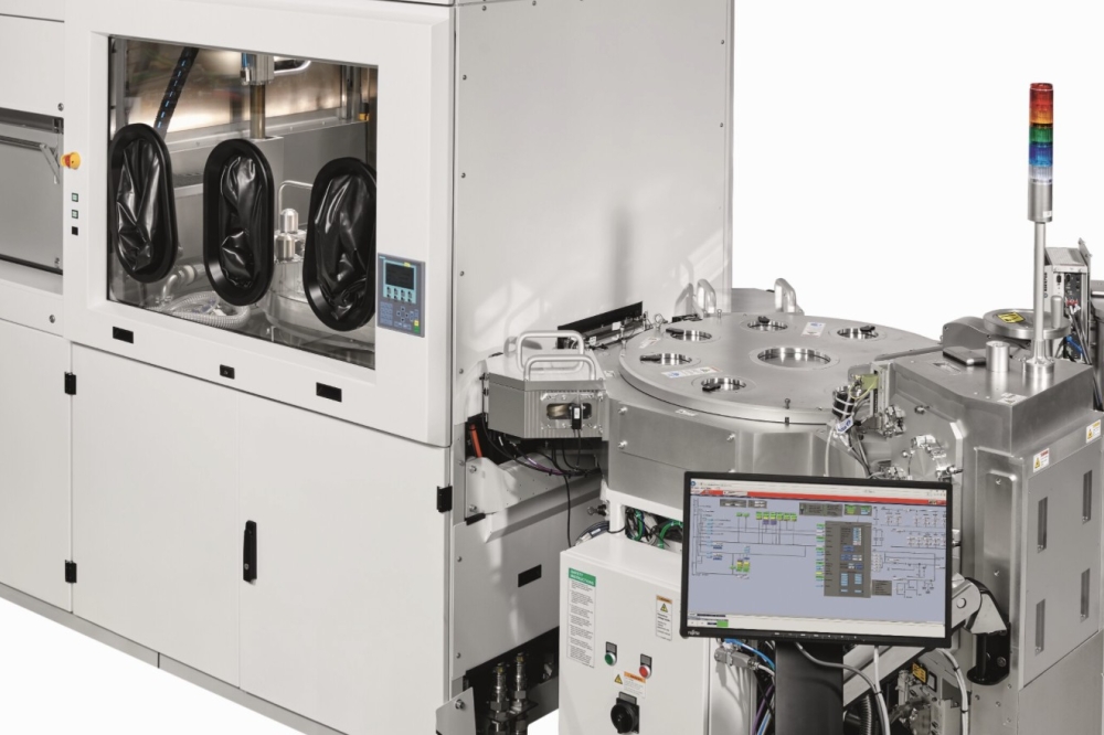
Pulsed MOCVD promises to improve AlN-based power devices
AlN has tremendous potential as a material for power electronics, with a key metric, the Baliga figure of merit, exceeding that for all other ultra-wide-bandgap semiconductors. However, device performance is held back by difficulties associated with doping, including high ionisation energies and the formation of self-compensating defects.
But much progress is possible by moving from conventional growth methods to pulsed MOCVD, according to a team of engineers from the University of South Carolina. These researchers are claiming that pulsed MOCVD enables more efficient doping of AlN, alongside a lower ionisation energy and superior doping control.
As the difficulties associated with doping AlN are well known, the nitride community has investigated a number of innovative techniques to try and address this issue. Efforts include the use of metal-modulated MBE, undertaken at low temperatures that reduce the formation of self-compensating defects; and the addition of a UV source during the MOCVD process, a solution that’s difficult to implement, but enables Fermi-level control and mitigates self-compensation. With the latter technique, silicon-doped AlN layers have a doping density of 2 x 1015 cm-3 and a mobility of 160 cm2 V-1 s-1.
The team from the University of South Carolina argues that their pulsed MOCVD is simpler to implement than that involving a UV source. Earlier this year they reported that switching from conventional to pulsed MOCVD enables an increase in the conductivity of AlN by an order of magnitude, and now they are demonstrating the capability of this growth technology for fabricating quasi-vertical Schottky barrier diodes.
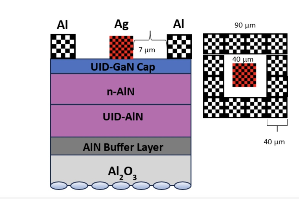
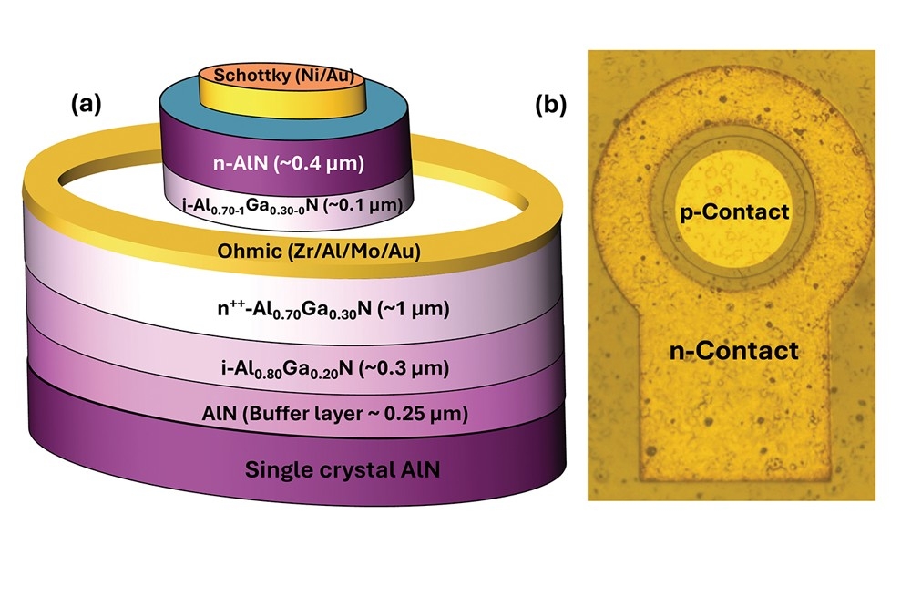
To produce these power diodes, the team began by taking an AlN substrate and using conventional MOCVD to grow a 250 nm-thick undoped AlN buffer layer, followed by an unintentionally doped Al0.8Ga0.2N layer, a 1 µm-thick silicon-doped Al0.7Ga0.3N layer for contact formation, and a 100 nm-thick undoped graded layer, with the aluminium mole fraction increasing from 70 percent to 100 percent.
Co-author of the paper detailing this work, Abdullah Al Mamum Mazumder, told Compound Semiconductor that they use conventional MOCVD for the growth of these layers, because it is capable of combining efficiency with high growth rates.
“To grow doped AlN layers, the use of pulsed MOCVD offers important advantages in terms of achievable dopant incorporation and smaller donor ionisation levels. This is why in this work we used pulsed MOCVD to grow the active AlN layer only.”
The engineers produced quasi-vertical Schottky barrier diodes with a circular geometry from their epiwafers. To form these devices, they used standard photolithography and inductively coupled plasma reactive ion etching to define mesas and access the Al0.7Ga0.3N layer – on this layer they formed the n-type contact, using electron-beam evaporation. Schottky contacts were added by electron-beam evaporation. This completed fabrication of the diodes, which had a 10 mm gap between the Schottky and ohmic contacts.
Electrical measurements revealed that the team’s Schottky barrier diodes have a breakdown voltage of around 395 V. According to simulations, the peak electric-field-breakdown is 9.9 MV cm-1. The engineers point out that incorporating passivation and field-plating would allow the electric field at breakdown to get close to the critical field for AlN – that’s 12-15 MV cm-1.
The team’s Schottky barrier diodes have a turn-on of around 2.2 V and an ideality factor of 2.4, due to oxide formation on the AlN surface and an imperfect metal-AlN interface. “We are planning to address these issues in our future work,” says team member Tariq Jamil.
Other goals include systematic studies of pulsed MOCVD growth of AlN and AlGaN materials with a very high aluminium content.
“Our tasks include increasing doping levels, material quality optimisation, and mobility and current transport analysis and optimisation,” says Mazumder. “We are also working on developing new devices using pulsed MOCVD. These include vertical and quasi-vertical Schottky and p-n diodes, as well as transistors.”
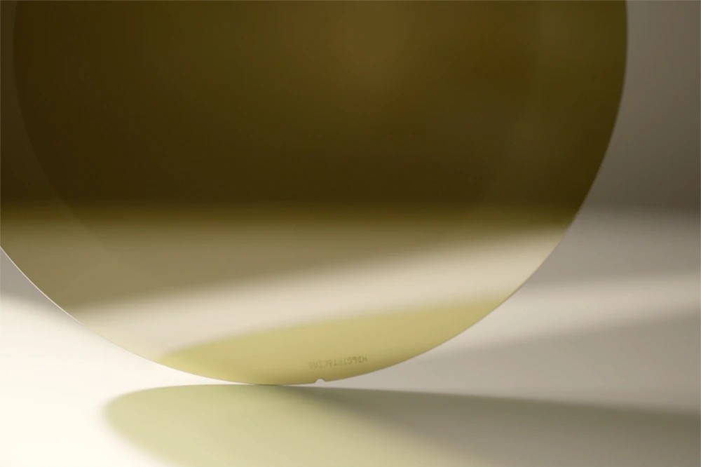
Pictured above: Engineers from the University of South Carolina have demonstrated the prowess of pulsed MOCVD for AlN growth by using this technology to produced quasi-vertical Schottky barrier diodes (a). The top view of the fabricated device (b).
Reference
A. A. M. Mazumder et al. Appl. Phys. Express. 18 065501 (2025)