Allos CTO challenges some common GaN-on-Si myths

Why carbon-doping is not necessary for high isolation and why interlayers are not a source of leakage
Allos Semiconductor's co-founder and CTO Atsushi Nishikawa has challenged a number of widespread beliefs about GaN-on-Si processes at the recent International Conference on Nitride Semiconductors (ICNS-12) in Strasbourg, France.
In his presentation 'Low vertical leakage current of 0.07 µm/mm2 at 600 V without intentional doping for 7 µm-thick GaN-on-Si', he questioned the idea that carbon doping is inevitable and that using interlayers in the buffer is a source of leakage. He also challenged the idea that the choice of the right reactor hardware is decisive in achieving good results.
Developers of GaN-on-Si epiwafers find that the crystal impurities from the growth process cause the isolation of GaN to be far below its theoretically possible values. To overcome these insufficiencies makers of GaN-on-Si epiwafers usually apply carbon doping to achieve the required isolation. Unfortunately, conventional methods of carbon and other doping have negative side-effects.
In contrast, Nishikawa says that Allos' results prove that by focusing on superior crystal quality and thick GaN layers the required low leakage currents can be accomplished without any intentional carbon or other doping. This not only avoids negative side-effects of doping but also widens the process window for further optimisation of numerous manufacturing and electrical properties.
Nishikawa also gave experimental evidence that interlayers are not a source of leakage, but quite the opposite. He showed that carefully controlled interlayer growth conditions and positioning of the interlayers can improve isolation by more than one order of magnitude.
In combination,he says, these techniques allow Allos to achieve a very low vertical and lateral leakage current of only 0.07 µA/mm2 and 0.005 µA/mm respectively at 600 V. This is based on 7 µm thick GaN with very high crystal quality of 316 arcsec for (002) and 413 arcsec for (002) XRD.
In the closing part of his presentation Nishikawa questioned whether the choice of the right reactor hardware would be decisive. Of course, good hardware matters, but is by far not the dominant factor.
Allos can apply its structure and growth methods on several hardware platforms as a comparison of results from two leading multi-wafer MOCVD reactor models demonstrates. On both reactors, similar material and electrical properties have been achieved.
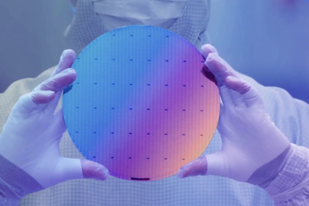
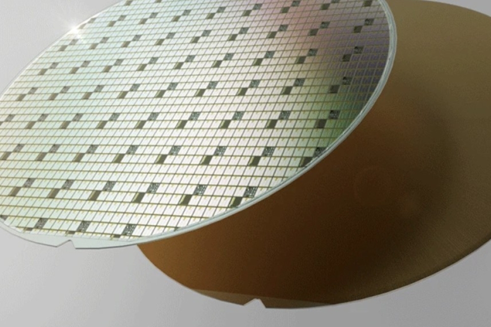
Allos' technology is available on both 150 mm and 200 mm epiwafer diameter, with SEMI-standard thicknesses. It is designed for manufacturability, is suitable for standard silicon lines, has a controlled minimum bow and no cracks.


