GaN blossoms into full technology solution

GaN devices, both discrete and integrated, are becoming more and more
available targeting an ever-increasing range of applications.
BY DR DENIS MARCON, GENERAL MANAGER, INNOSCIENCE EUROPE
NOT SO LONG AGO, gallium nitride (GaN) technology was considered to be suitable only for specific applications in RF and microwave and other specialist markets. The first and still largest commercial usage of GaN for power switching applications is to be found in compact mobile phone chargers, where the emergence of the USB-PD standard and market pressure for sleek accessories created a demand for higher power density. It could be said that the GaN industry ‘grew up’ with this market, learning how to deliver large volumes of parts. But now the GaN industry is transitioning again with the emergence of a wide variety of GaN devices, both high and low voltage and – recently – by adding integrated solutions as well as discrete HEMTs.

Figure 1: Astonishing power density specs can be achieved using GaN in both the primary and secondary PSU sides.
It’s probably worth spending a paragraph highlighting just what all the fuss is about. Simply, GaN delivers higher power, higher power density and greater efficiency with almost zero switching losses. This is mainly due to two factors. First, the accepted industry benchmark Figure of Merit, Ron Qg, is 10 times better than silicon. This means that systems can switch at a higher frequency without incurring any loss in efficiency. This gives designers the freedom to use smaller passives, which can result in reducing the overall BOM cost (more later). High efficiency also means that less heat is generated, so thermal management solutions such as heatsinks and fans can be eliminated or reduced in size.
The second aspect of GaN is that it has no body diode, and therefore the reverse recovery current is zero. This allows designers to select simpler power conversion topologies; for example, the totem pole bridgeless PFC design can be used instead of the more complex, larger BOM, dual boost bridgeless PFC circuit which would be necessary to keep efficiency high if the design was restricted to using even the best silicon MOSFETS.
In order for GaN to succeed in a wide range of application fields, industry needs a correspondingly wide range of GaN devices.

Figure 2: Using GaN results in a sleek design for LED driver and 6W
power saving/track. At the bottom, a side by side comparison of a 200W
GaN solution versus a 120W Silicon is reported.
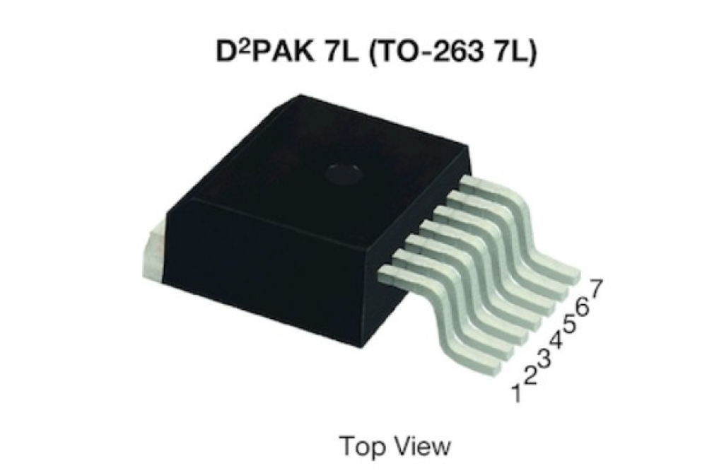
Innoscience, the world’s largest 8in GaN-on-silicon integrated device manufacturer (IDM), now offers a very wide portfolio of GaN power devices covering low, medium and high voltage applications, with low voltage parts spanning 30 - 150V with ON resistances as low as 1.2mΩ. High voltage devices are available up to 700V with RDS(on) values between 30 - 600mΩ. These GaN FETs are also available in different packages including wafer level CSP to flip chip QFN with a top- or bottom-side side cooling DFN, TO- etc. By offering many standard packages, designers that are familiar with those packages from using silicon devices can easily switch to GaN. Also very recently, we have introduced a single- channel gate-driver optimized for GaN solutions.
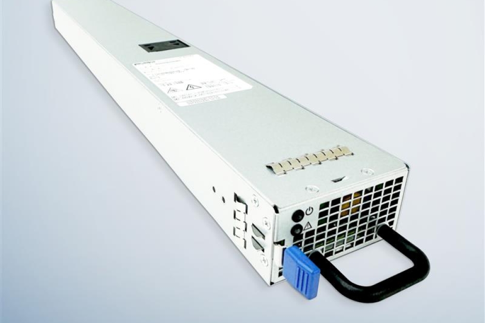
As an example of what can be achieved by combining low and high voltage GaN devices within a power supply unit (PSU) is considered in Figure 1.
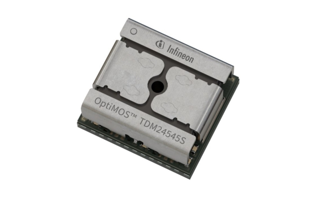
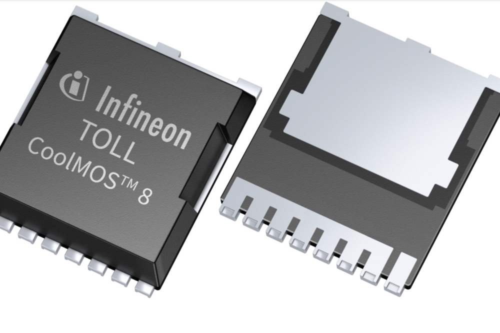
This example shows a 4.2 kilowatt PSU using a 700V high voltage GaN part on the primary side in combination with a 150V GaN device on the secondary side. The figure details a totem pole PFC plus LLC design using 30mΩ RDS(on) and 70mΩ RDS(on) high voltage GaN power switches in the TOLL package for the primary side; and for the secondary, four pairs of 3.2mΩ RDS(on) low voltage parts in a flip chip QFN package.
The result is a 4.2kW PSU that measures just 185 x 69 x 37mm and achieves an astonishing power density of 130 watts per cubic inch. It easily meets the 80 Plus titanium rating for efficiency, peaking at 97.5%. The equivalent PSU made using silicon could easily be twice the size.
Figure 2,F shows another application ideally suited to GaN. In a 150W tracklight, a silicon-based LED-driver is either too long or two fat. With GaN, you can have a 200kHz PFC plus LLC solution measuring 15 x 15 x 200mm that fits perfectly in the fixture. Plus, the Innoscience solution is 4% more efficient, resulting on a saving of 6W/track.

Figure 3: Many applications can benefit from GaN.
Moreover, a direct comparison of a 200W GaN solution versus a 120W Silicon solution is provided at the bottom of Figure 2, which shows that the GaN solution is 37% shorter and 57% thinner than a Silicon solution.
There are many other examples (Figure 3): a 300W TV, where a chunky power supply would spoil the profile of the otherwise slender unit, now powered by a GaN-based solution measuring 220 x 180 x 8.5mm; a 1000W DC/DC converter that is 70% smaller and more efficient than a 600W silicon unit; the ubiquitous 20 – 240W charger designs; and many others for inverters, motor drivers, photo-voltaic solar power etc.
So far, we have only looked at discrete GaN solutions which are preferred by many engineers because of their design flexibility. However, using GaN does require some design know-how – which is readily available – as well as a GaN driver, protection circuitry and other components such as a sense resistor to read out the current (Figure 4).
Whilst this is perfectly viable solution for many applications, Innoscience is introducing a range of integrated solutions for designers that say that they just want to use GaN and reap the benefits as simply as possible. SolidGaN devices combine power transistor, driver, current sense and other functions within a single, industry-standard QFN 6x8mm package. The 700V ISG610x devices cover the range from 140 to 450mohm, and save PCB space and BOM count, while increasing efficiency and simplifying design for applications including USB-PD chargers, LED lighting, AC/DC and DC/DC power supplies and PFC, QR flyback, ACF, half bridge, and full bridge circuits. The integrated devices feature a wide 9-80V VCC range which is beneficial in USB-PD applications that require up to 28V output.

Figure 4: The discrete GaN schematic.
For low power operation, ISG610x family ICs also feature a low, 115µA quiescent current, thanks to an innovative automatic standby mode which is activated when the PWM signal voltage remains below VPWM_LO for a certain time period.
During this time, most of the internal circuitry is turned off, dramatically reducing energy wastage, enabling devices to meet the No-Load, Low-Load specifications of regulatory bodies such as ENERGYSTAR.
The loss-less current sensing with 7% accuracy of the new SolidGaN devices offers several benefits. Firstly, because the current sensing resistor loss is eliminated, a larger RDS(on) can be accommodated with no loss in performance, leading to cost reduction. Secondly component count is reduced and PCB footprint is minimized. Devices also feature a programmable switch turn-on slew rate to enable EMI to be minimised. An internal linear voltage regulator is included to assure a 6.5V supply, maximizing power efficiency while ensuring the reliability of the GaN HEMT. Finally, built-In under-voltage lock-out (UVLO), over-current (OCP) and over-temperature (OTP) protection are incorporated within the IC.

Figure 5: New integrated GaN ICs from Innoscience are easy to use.
Price and reliability
With such significant benefits and wide availability in an ever-increasing device portfolio to match new application, one might be tempted to wonder why any design team would not make the move to GaN. The answer is simple, but based on outdated misconceptions concerning price and reliability.
Based on publicly available data, Figure 6 shows that Innoscience’s InnoGaN GaN HEMTs are now price competitive with silicon. Furthermore, GaN offers the possibility to save further costs at a system level because the increased efficiency will lead to a reduction in size – and therefore price - of the passives and magnetic components that will be required.
Innoscience has managed to achieve price price-competitive GaN devices by investing in the world’s largest 8in GaN-on-Si fabs, thus leveraging massive economies of scale. Also, by controlling all key manufacturing processes, including epitaxy, in house, the company is achieving consistently high yields.
If we now turn to reliability, the first point to make is that GaN may seem to be new, but on fact it has been around for over 20 years and is well studied and understood. Devices are now tested to the international JEDEC standard and to specific
JEDEC guidelines drafted for wideband gap devices (JEP 180) where devices are stressed under switching stress to mimic real application usage.
Innoscience performs further extrapolated lifetime tests including HTGB (beyond max gate specs) and HTRB (beyond max off-state drain voltage specs).

Figure 6: Comparing the price of SJ devices and InnoGaN.
Conclusion
GaN devices, both discrete and integrated, are becoming more and more available targeting an ever-increasing range of applications. With GaN devices power conversions and power management solutions can be made smaller, lighter, more efficient and simpler (less BOM). Devices are proven to be reliable, and – certainly with Innoscience’s devices – there is no cost penalty to be paid by moving to GaN, quite possibly the reverse.