Enabling test automation in new power electronics reliability
Test automation is critical for optimizing reliability testing of power
semiconductor devices during all stages from R&D to Manufacturing.
By Andrea Vinci, Senior Technical Marketing Manager at Tektronix.
There is no such thing as a univocal meaning and definition for “reliability” testing. The definition I like the most is this one: a methodology to discover how to improve product quality, enabling you to verify whether your device can withstand all possible stresses it will face once marketed into a customer’s application.

Figure 1: Semiconductor Product Development Phases
There are several development stages where reliability testing is critical: the R&D (Research and Development) phase, the pre-production (small quantities) phase, and in the mass production phase. In R&D, it is important to ensure that the characteristics and reliability defined in the design phase are met. In Pre-Production, the mass production line is used in limited lot sizes to evaluate and exclude problems before mass production commences.
The Bathub Plot
Ask reliability engineers to draw a function on a graph, and they will certainly come back with a bathtub curve like the one in Figure 2; the curve depicts a number of temporal regions for device failures.

Figure 2: The Bathtub Plot
Depending on the product lifecycle stage, reliability tests can present different challenges, methodologies, intrinsic constraints. Mainly, they will reveal different failure modes. You refer to an “extrinsic” reliability indicator when you test robustness against failures related to defectivity and process variability, causes that are external to the real capabilities of the design and materials. You refer to an “intrinsic” reliability of the compound semiconductor when the failure is related to how the component is designed (device structure, materials, and their wear out).
In summary, devices need to be stressed to failure and failure modes, analyzed as well as categorized as either extrinsic (early life failure) or intrinsic (wear-out failure). When you will have fixed the extrinsic failure causes, then primary failures will be due to intrinsic sources; this is when you need to model how the wear-out occurs. The degradation model will help you to predict lifetime and failure rate.
We all agree it is really not possible to wait years to study how a new technology-based compound semiconductor device can fail. To accelerate a potential failure mechanism, an enhanced stress is applied to devices, which, in the case of WBG power semiconductor devices, can mean stressing current, voltage, temperature, humidity, mechanical vibrations etc.Applying specific degradation models is the way to predict failure rates under stated stress conditions and lifetimes.

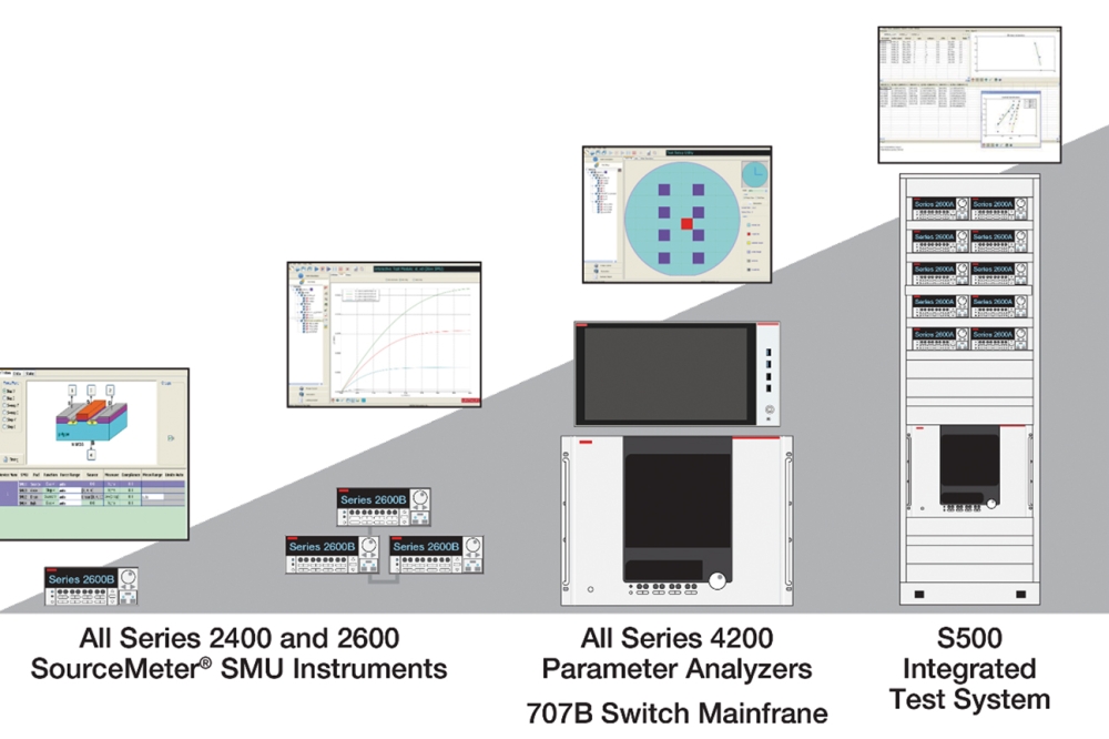
Figure 3: From lab to fab with same equipment building blocks
Meeting Application Related Standards
Everyone agrees today about how wide bandgap (WBG) semiconductors like SiC and GaN, thanks to their superior electrical and thermal characteristics compared to silicon, have enabled the transformation of electricity use especially for power electronics switching applications. They are the de-facto building blocks of power converters in use across electrified mobility market, data centers, renewable energy and electric grids etc. When used in high-voltage, high-power or high-temperature conditions, all new switching devices experience electrical and thermal stresses because of high electric fields and high currents generated during their operation. New technologies like WBG can demand more extensive and accurate approached than standard guidelines.
Every market, depending on its specificity, demands component suppliers to guarantee specific operation conditions. As previously stated, manufacturers do this by testing devices extensively for reliability. The approach to guarantee reliability is to follow application specific guidelines and standards.
There are reliability assurance guideline for space applications applying to compound-semiconductor such as GaAs, which are typically used in that Industry. In contrast, the automotive industry typically uses SiC discrete MOSFETs; to qualify them at their determined operating voltage levels (e.g. 1200V or 1700V) and max operating temperature levels (e.g. 175 °C or above) suppliers must follow the Automotive Electronics Council AEC-Q101 standard guideline. Other standards like JEDEC are for industrial use of the component’s qualification, MIL-STD-xx for military and so on.
Approaching new technologies adoption
Failure mode scenarios for new compound-semiconductors based power electronics can be multiple and complex, and all need to be addressed to ensure a very low failure rate percentage with significantly high statistical confidence. The so-called physics for failure analysis is getting increasingly complex with wideband gap materials as are predictions on their behavior under extreme environmental conditions.
Qualification tests where accelerant stresses are applied have different names.
HTRB stands for high-temperature reverse bias test; this test aims to analyze failure related to DC bias stress of Vds on a MOSFET. TDDB stands instead for time-dependent dielectric breakdown; it is a failure mode that can occur when a conduction path is formed by an overlapping of defects generated in the dielectric of the MOSFET.
A GaN HEMT is usually under a high forward bias voltage stress which is not only DC but also AC. AC stress shows longer breakdown times than under DC stress and it varies a lot with higher switching frequency condition, temperature, etc.
Taking these tests in an exhaustive way requires the running of hundreds of thousands of hours of testing, each with tens of thousands of temperature cycles and humidity points. Post qualification, semiconductor manufactures still need to accumulate millions or trillions of hours data to acquire a failure in time (FIT) rate in the field.
We then need reliable and accurate measurement logging to complete our lifetime prediction modeling and release the fundamental calculation called mean time to failure (MTTF), which is the output of a prediction modeling algorithm fed by data obtained with test methodologies like the TDDB.
Time invested on reliability testing can be significant. Test execution speed and amount of information on reliability to be obtained need to be balanced, and deciding what to prioritize as the most important is difficult.
The Ask to T&M Suppliers
Test and Measurement Suppliers equipment must meet the need of customers to follow ever more demanding standardized methods for performing reliability testing and failure analysis at the packaged device level,; as well as within manufacturing where these tests are run at wafer level.
In both contexts, factors like testing time and measurement capabilities directly correlate to production capacity, testing cost and material loss if the packaged device fails;the optimization process of testing closely relates to the ability to evolve test automation.
Semiconductor manufacturers producing high quality devices seek suppliers of reliable sources, to apply the electrical stress in both static and dynamic conditions, and accurate measurement at the same time remarkably high or extremely fast, or both dv/dt or di/dt. Reliability test infrastructure needs equipment capable of sourcing voltage and current ranges at the highest testing capacity but with the minimum cost and requirement on the sourcing equipment. Precision is accuracy and repeatability in both the parameter adjusting, cycle after cycle, and measurement.
Further need is to continuously monitor and display measured thermal and electrical signals, providing an easy to configure control panel to quickly upload electrical and thermal stress scenarios with the minimal cost of ownership for data acquisition and monitoring systems.
A Real Packaged Device Reliability Use Case Scenario
How do you account for the longer potential lifespan of SiC based devices? They are subjected to as much as ten times the operating voltage as their silicon predecessors, and likely operate in high temperature environments. Typical SiC MOSFETs reliability tests involve stressing a batch of sample devices for hundreds or thousands of hours with bias voltages, that are greater than or equal to their normal operating voltages, while subjecting them to temperatures that are well beyond normal operating conditions. During this stress, a variety of key operating parameters are measured at specific time intervals. Changes in device performance may indicate a defect in the part, allowing it to be pulled for failure analysis before it gets to the end user.
A multi-channel, programmable power supply can be used to power and stress the device. The channels of the power supply can be routed together in series, or parallel, to increase the voltage or current output of the supply. Programmable power supplies, that have sweeping functionality, allow you to customize the stressing routine to fit your testing needs. Batches of devices can be connected in parallel to a single supply to increase test density.
On the measurement side, DMMs provide options to choose the level of accuracy and resolution that you need with either a 6½-digit or 7½-digit meter, but also have switching capabilities, increasing the number of devices that can be tested at a given time and decreasing overall test time. Multi-channel DMMs are great tools to monitor temperature, as well, during temperature-controlled tests.
Software that controls the whole solution can ease integration and setup by automating the process. The software should be able to collect data for extended periods of time, ensuring you can view trends in the devices.
Keithley’s KickStart Software ties the whole solution together, with intuitive controls and long-term data collection.
Keithley KickStart software can control and configure each of the power supply channels individually, output a constant bias voltage for stressing or customize the output sequence using the list sweep function. The sweep points can be defined directly in KickStart software or by importing a ready-made CSV file. The time for each point in the sweep is controlled by the list hold time setting. Setting this to Points sets up several measurements to take per step in the sweep. Changing this setting to Time allows you to set a custom dwell time in seconds for each step, truly customizing the stress sequence applied to the device.
A Real Wafer Level Reliability Use Case Scenario
Let us now consider the case of testing before device packaging occurs, hence at wafer level. Engineers need to deploy tests such as charge trapping, NBTI enhanced hot carrier and TDDB enhanced NBTI. Measurement methodology requires DC stress and measurement to a point where both DC and pulse stress are used to study degradation relaxation effect.
Keithley instrumentation ranges across the 4200A-SCS device characterization system Keithley 2600 Series and 2400 Series SMUs, ultra-sensitive current sources and nanovoltmeters, switching and data acquisition systems.
These building blocks are easy to integrate into existing reliability, technology development, and semiconductor labs, incorporating them into a self-contained and fully automated test system.
Many of these instruments come with Test Script Processor (TSP®) and TSP-Link® technology for ultra- high-speed operation and parallel test, enabling the instrument to perform advanced tests without PC intervention using embedded test scripts and complete test subroutines. Keithley instrumentation includes a comprehensive device characterization suite called ACS (Advanced Characterization Suite); this software supports component characterization testing of packaged parts and wafer-level testing using probers.
The software embeds generalized libraries, functions, and demo projects to support the Shared Stress Reliability Test Application. Test libraries based on JEDEC Standard (e.g. JEP183A for the Power MOSFET SiC Reliability test) are included as well.
At the wafer level, Keithley’s ACS integrated test systems feature a Wafer Description Utility and wafer map. Users can easily build wafer description files with integrated test plans. Color-coded wafer maps are updated in real-time during test execution to show pass/fail metrics, providing clear visibility into test results and assuring that test outcomes will be productive.

Figure 4: ACS standard suite for interactive probe station control
There is interactive prober controller to control wafer movement during test development to validate test setups on actual structures and during lot disposition to navigate to a problem area of the wafer and execute testing manually. ACS supports control of FormFactor, MPI, Electroglas, TEL and ACCRETECH, Signatone, Semiprobe, HiSOL and other probers.
ACS includes test routines such as macros, scripts, and custom GUIs. You can control any Test Script Processor (TSP™) instrument using a script test module (STM) script, but also using the Python language test module (PTM) script, including instrumentation from other vendors.
To increase throughput while minimizing costs the system supports shared stress testing in ACS software v6.3, allowing users to apply different reliability test methods such as TDDB, AC-TDDB, TZDB, and HTRB to large groups of DUTs in parallel. A switch matrix is used to control when stress is applied to the DUTs and when measurements are taken.
A Typical SiC MOSFETs Reliabliity Issue
JEDEC standard JEP183A introduced guidelines for measuring the threshold voltage (Vt) of an N-channel vertical structure SiC MOSFET device. This was because SiC devices present in general an higher instability of Vt compared to Silicon. The standard aimed to identify measurement methods and propose preconditioning guidelines to minimize the effect of Vt hysteresis.
This hysteresis phenomenon is mainly caused by hole charge trapping occurring when sweeping the gate device upward and downward. The JEP183A standard proposed then a new guideline to measure threshold voltage in a more consistent way. The idea is to add a pre-conditioning pulse prior to the gate sweep measurement to release any trapped hole charges from the silicon oxide interface and sweep downward. The JEP183A standard also proposed three different methods of SiC threshold measurement.
Keithley systems based on SourceMeter® units (SMUs) implement this threshold voltage test on SiC Power Mosfets devices. SMUs and software can support all three of the methods proposed by the JEDEC standard.
The procedure with pre-conditioning pulse and sweeping can be easily done by TSP scripts to run on instrument or that can be embedded in ACS-Standard and ACS-BASIC software, giving the user the benefit of ACS’s graphical interface so code modification is not necessary.
Conclusion
Test automation is critical for optimizing reliability testing of power semiconductor devices during all stages from R&D to Manufacturing.
For maximum system speed and programming simplicity, the Keithley TSP-Link® intercommunication bus allows multiple building block instruments to trigger and communicate with each other. Keithley Test Script Processor (TSP) technology enables all instrument control and most data management to be performed at the instrument level, eliminating the typical LAN traffic delays that slow system-level throughput in instrument-based systems.

Figure 5: Python script for time-dependent dielectric breakdown (TDDB) analysis
ACS software provides all the tools required for shared stress reliability testing and makes automating the tests easy. Along with embedded projects, a new PTM (python test module) library and linear parametric test library (ptmlpt) have been implemented as well. The PTM can be modified by the user as needed, showing that ACS software offers the flexibility to support almost any reliability test application.