Silicon-based semiconductors – powering ahead

Silicon-based semiconductor technologies, such as power MOSFETs and
IGBTs, are essential in every modern power electronics system and play a
crucial role in controlling and converting electrical energy. Due to
their unique physical properties, these specialized electronic
components are designed to handle high voltages and currents, providing
benefits and advantages in many different applications, such as
renewable energy systems, electric vehicles, power supply for data
centres and industrial machines.
BY ANTONINO GAITO, POWER TRANSISTOR SUB-GROUP, TECHNICAL MARKETING MANAGER, HIGH VOLTAGE DIVISION, STMICROELECTRONICS AND CARMELO FINOCCHIARO, POWER TRANSISTOR SUB-GROUP,
MARKETING ENGINEER, STMICROELECTRONICS
A power MOSFET (Metal-Oxide-Semiconductor Field-Effect Transistor) is a type of Field-Effect Transistor (FET). Applying a voltage to the gate terminal, a current will flow through the channel from the drain to the source.
Among the main parameters which affect the most performance of a MOSFET, there are the drain-source resistance RDSon, the gate charge Qg and the breakdown voltage BVDss. In terms of efficiency, lower RDSon means lower conduction losses and higher efficiency in applications where MOSFETs are used to switch current on and off. Lower RDSon also means less heat will be generated during operation, which can reduce the need for heat sinks and other cooling mechanisms. In high-frequency applications, the switching losses might become more significant compared to conduction losses, but having a low RDSon is still beneficial for the overall device performance.

Figure 1 Power transistors technologies.
A lower gate charge allows faster switching speeds, and this is advantageous in high-frequency applications. When a switch commutes, power is dissipated in the form of heat. A lower gate charge can reduce these losses, improving efficiency. The gate charge also determines the current needed from the gate driver to switch the MOSFET at desired speeds. Lower gate charge can lower the requirements on the gate driver circuit.

Figure 2 Planar MOSFET technology.
The breakdown voltage helps determine the maximum voltage that the system can handle. MOSFETs must be chosen with a breakdown voltage higher than the maximum voltage expected in the application. A higher breakdown voltage also provides a larger safety margin, improving the reliability of the MOSFET under transient conditions. Power systems often experience voltage spikes, and having a sufficient breakdown voltage helps protect against these transients. The evolution of silicon MOSFETs from planar to superior structure technology represents a significant advancement in semiconductor design. Planar MOSFETs have a simple structure and are cost-effective for low-power applications, but they face limitations in terms of voltage scaling and drain-source resistance.

Figure 3 High Voltage Silicon MOSFET technology evolution.
A super-junction MOSFET is designed with a more complex structure that includes a series of p-type and n-type regions that are alternately stacked vertically in the drift region, between the gate and the drain. The key factor of the super-junction design is the charge balance between these p-type and n-type regions, which allow for much higher doping concentrations while maintaining the breakdown voltage at the same level. Due to the higher doping levels and the charge balance, super-junction MOSFETs have significantly reduced drain-source resistance compared to that of planar MOSFETs with the same voltage rating. These characteristics enable the ability to handle higher voltages without increasing the physical size of the device, leading to higher efficiency, especially in high-voltage applications. The manufacturing process for super-junction MOSFETs is more complex and requires more precise control than that of planar MOSFETs. Planar MOSFETs are often used in low to medium voltage applications, while super-junction MOSFETs are preferred for high-voltage and high-efficiency applications. In conclusion, the super-junction MOSFET showcase, in addition to a higher dopant concentration, multiple benefits as lower a lower RDSon, improved thermal impedance or the possibility to use the die in thinner packages.

Figure 4 From planar to super-junction structure.
Improvements have been made not only to the structure but also in the mechanical performance using a different top passivation. The top of the structure is subjected to electrical and mechanical stress. The passivation process is responsible for protecting the active structure from mechanical stress, ensuring it remains isolated. In the past, a simple Nitride layer was used for this purpose, but the interactions with the metallization layer generated some mechanical stress, leading to die cracks. A solution to reduce this impact was the use of an additional layer made with TEOS (Tetraethyl Orthosilicate). Today, the latest super-junction structures complete the top of the die with an extra layer of polyimide.
The better performances, both in conduction and dynamic commutations of the latest super-junction structure, enable the achievement of high efficiency, saving energy, and maximizing power conversion. For example, as shown in Figure 5, the latest super-junction technology can generate an improvement of 0.5%. Although this improvement may initially seem negligible, it is significant when the power level is high. In fact, saving 0.5% in a 10W power system means only 50mW, but the same ratio becomes more significant when we refer to systems that manage kilowatts (kW), like solar converters or automotive power converters.

Figure 5 Application test and analysis of different devices, comparing main parameters.
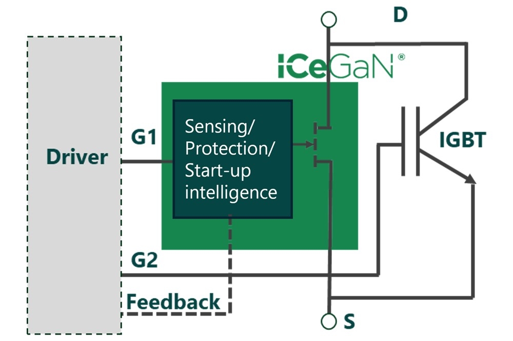
To complete this overview, it is fundamental to take a look to the Insulated Gate Bipolar Transistor (IGBT), a semiconductor device that is widely used in power electronics. It combines the simple gate drive characteristics of a Metal-Oxide-Semiconductor Field-Effect Transistor (MOSFET) with the high-current and low-saturation-voltage capability of a bipolar transistor. The IGBT is designed to handle large power levels and is commonly used in applications such as variable-frequency drives (VFDs), electric cars, trains, variable-speed refrigerators, air-conditioners, and even in the power grids for switching or adjusting reactive power. Below a short overview of the different IGBTs topologies is made to show the main differences between them.
Non-Punch-through is the first IGBT technology and has higher saturation voltage VCEsat, slower turn-off speeds and a positive temperature coefficient, meaning that as the temperature increases, the on-state voltage also increases. Punch-through (PT) IGBTs, conversely, can also exhibit a positive temperature coefficient at higher current levels, which can be advantageous for parallel operation, as it helps to prevent thermal runaway. The buffer layer in PT IGBTs indeed reduces the minority carrier lifetime, which results in faster turn-off speeds and lower switching energy.
The Trench PT presents a different structure because it has a vertical inversion channel of the p-type emitter region (while in the previous planar topologies is horizontal), which means that the JFET effect present in planar gate IGBTs (which limits current flow) can now be reduced. By having a vertical channel, the trench gate IGBT enhances conductance modulation efficiency near the emitter region due to the high electron injection, which improves the device's overall performance.

Figure 6 IGBT technology.
The Trench Field-stop (FS) IGBT is a type of IGBT that combines the benefits of the trench gate structure with those of the buffer layer. This design aims to provide faster switching speeds and lower on-state voltage drops compared to conventional IGBTs. The Field-stop (or buffer) layer is a highly doped n-type region located just below the n- drift region. It is designed to stop the electric field from extending into the thick n- buffer layer, which allows for a thinner drift region without compromising breakdown voltage.
The Hole barrier (HB) IGBT is basically a Trench FS which also comprises an additional n-layer to increase the conductivity in the upper-layer zones. This provides a higher VCEsat, improving the turn-off behavior and reducing the tail currents. By managing the movement of electrons within the device, Hole barrier IGBT can achieve faster switching speeds and lower losses, making them suitable for applications where efficiency is critical.

Figure 7 The Hole barrier structure.
The ability to withstand hard stress, such as a short circuit, is a critical feature for many applications, particularly in power electronics where unexpected short circuits can occur for various reasons, such as rotor blockage or component failure. To address this requirement, different strategies are implemented into the IGBT structure. One such strategy is the generation of dummy cells. These cells do not participate in the conduction of the structure, allowing it to sustain higher short circuit current values. The trade-off is a lower saturation current and lower current density. This strategy balances the need for short circuit robustness with the impact on performance.

Figure 8 Trench layout strategy.
The term "narrow mesa" in the context of Trench Field Stop (FS) IGBTs refers to the design of the area between the trenches where the gate oxide and field stop layer are located.
In a Trench FS IGBT, the gate electrode is embedded in narrow trenches etched into the silicon. The space between these trenches is known as the mesa. A narrow mesa means that the distance between the trenches is minimized. This design allows for a higher cell density, which can increase the current-carrying capability of the device and reduce on-state resistance (RDSon). The Field-stop layer is optimized to prevent the electric field from extending too deeply into the device, which helps to maintain a high breakdown voltage with a thinner drift region.

Figure 9 Improvement from Trench Field-stop to Narrow Mesa II.
The narrow mesa design is part of the overall structure that contributes to the improved performance of Trench FS IGBTs, offering benefits such as lower conduction losses and faster switching speeds compared to traditional planar IGBTs. When referring to "Narrow Mesa II" or "Generation II" in the context of IGBTs, it likely indicates an evolution of the trench IGBT technology where the narrow mesa concept has been further refined or optimized. Manufacturers often release different generations of IGBTs with improvements in the cell design, trench technology, and other features to achieve better performance. In terms of advantages, Generation II Trench IGBTs over Narrow Mesa showcases lower on-state resistance, and faster switching characteristics lead to higher efficiency in power conversion applications. They also possess the ability to handle higher currents in a smaller area makes these devices suitable for compact designs. Finally, improved efficiency results in less heat generation, which can simplify thermal management requirements.
Power electronics has seen significant advancements over the last years, driven by the need for more efficient, compact, and reliable power conversion systems, and their evolution will likely be determined by the specific requirements in the considered application. Integration and hybrid approaches may also emerge, where silicon is used alongside wide-bandgap materials to optimize performance and cost. Additionally, advancements in silicon technology may extend its viability in certain high-performance areas.