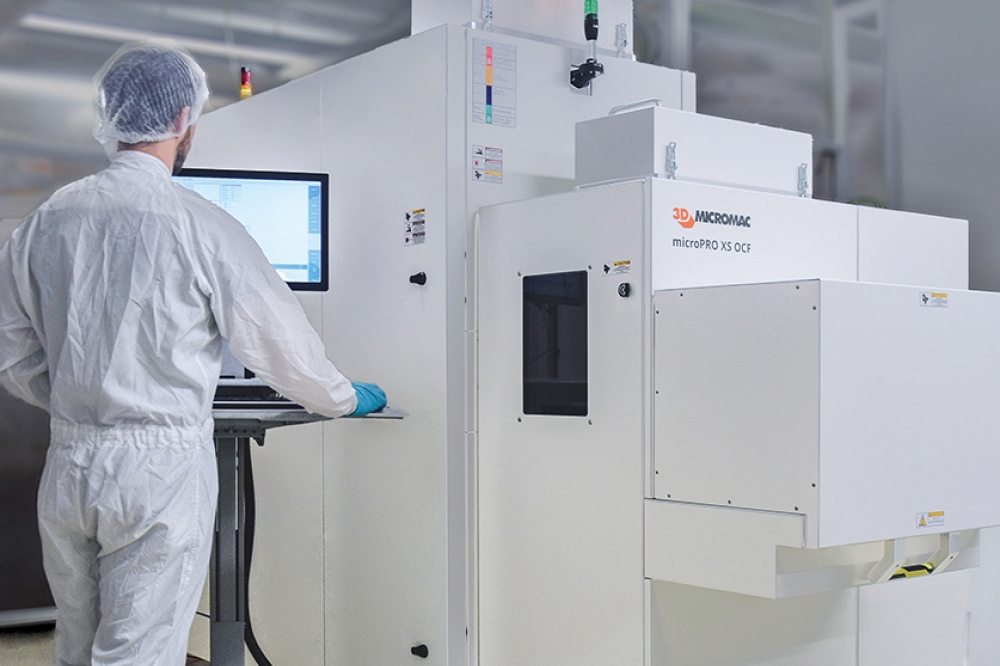
Revolutionising power: the impact of laser-based ohmic contact formation in SiC semiconductors
The realm of power electronics is witnessing a paradigm shift with the
advent of silicon carbide (SiC).
BY 3D-MICROMAC
The realm of power electronics is witnessing a paradigm shift with the
advent of silicon carbide (SiC). SiC is especially advantageous for
applications in electric vehicles, renewable energy systems, and
high-voltage power transmission.
A pivital factor in harnessing these advantages is the Ohmic Contact Formation (OCF) process, especially for 4H-SiC power semiconductor devices with their complex vertical structures. Efficient backside processing, which is integral to OCF, is a critical aspect in ensuring the operational efficacy and reliability of these devices.
The basics of ohmic contact formation OCF is a fundamental yet complex process in the manufacture of semiconductor devices. It involves the creation of metal contacts on the semiconductor material, facilitating efficient current flow. For SiC devices, OCF is a challenging endeavor due to the material’s inherent properties. The conventional approach typically involves the application of nickel or titanium layers. This process facilitates the transition from Schottky to Ohmic contacts, which is essential for efficient device operation. However, the traditional OCF methods, including high-temperature annealing, pose significant challenges. They often lead to contact degradation, increased stress on the device and limited electrical properties, particularly in thinner SiC wafers, thereby necessitating more innovative and delicate approaches.

Figure 1: The Ni-layer is annealed by exposure to laser
radiation forming an ohmic contact formation based on NixSiy.
Advancements in laser-based OCF
The evolution of OCF in SiC semiconductors has taken a significant leap forward with the introduction of laser-based techniques. This innovative approach stands in stark contrast to the traditional high-temperature annealing methods. Laser-based OCF utilizes specialized laser systems, such as those employing nanosecond pulses, to form Ohmic contacts with a high degree of precision and control. The key advantage of using laser systems lies in their ability to deliver targeted energy to specific areas of the semiconductor. This localized approach minimizes thermal stress and potential damage, a crucial factor for maintaining the integrity of thinner SiC wafers – especially when their front side has been already processed with heat sensitive electrical applications.

Figure 2: Flat top of laser spot
Impact on SiC-Ni interface and device performance
A study conducted by 3D-Micromac provides pivotal insights into the effects of laser-based OCF on the SiC-Nickel (SiC-Ni) interface, a critical aspect in the performance of power semiconductor devices.
This research is instrumental in demonstrating how advanced laser techniques enhance the efficiency and reliability of SiC devices, marking a significant advancement in semiconductor technology.
The study meticulously analysed the outcomes of using different types of lasers, including those with distinct beam profiles and pulse durations. The results clearly indicated that specific laser systems, particularly those with finely-tuned beam profiles and controlled energy output, were more effective in creating uniform and defect-free Ohmic contacts.

Figure 3: Parameters of Run 1
The key findings of the 3D-Micromac study revolve around the comparison of various laser systems and their impact on the SiC-Ni interface:
• Laser System Comparison: The top hat profile (see Figure 2), as used in 3D-Micromac’s microPRO XS OCF system, demonstrated lower forward resistance compared to the Gaussian beam process, indicating a more efficient OCF process.
• Impact of Wafer Parameters: Wafer thickness and the grinding process significantly influenced forward resistance. Thinner wafers showed reduced forward resistance, underlining the importance of precise OCF in thinner wafers.
• Laser Parameters Optimisation: Adjusting the pulse to pulse overlap and the pulse energy density was found to be crucial. Higher energy density or pulse overlap resulted in lower forward resistance, though it was possible to increase
throughput by reducing the overlap.
• Wafer Material Influence: Variations in dopant concentration within the wafer material affected the electrical characteristics, highlighting the need for uniform wafer processing.
•Front Side Structure Preservation: The study also confirmed that thermal laser annealing for OCF does not affect the surface structures, even with higher laser energy, making it suitable for thin wafers.

Figure 4: Distributions of forward resistance measurement on three wafer
types. a) Grinding A with 175 µm thickness, b) Grinding A with 80 µm
thickness, c) Grinding B with 175 µm thickness
For this study two wafer runs were performed on SIC wafers with vertical resistor structures.
The wafers had a thickness of 80 and 175 µm. In particular for this evaluation, low forward resistance was the main quality criterion. A reference process (system 1) with a single annealing parameter was compared with the 3D-Micromac process, for which a parameter sweep was performed. With this, the pulse energy density and the pulse overlap were varied (Figure 3).
Figure 4 shows the results of forward resistance measurements on three wafer types. As can be seen the vertical resistance depends mostly on the substrate thickness, but also the grinding process. The overall aim is to reduce vertical resistance. Following Ohm’s law, a reduction in resistance leads to a decrease in the required forward voltage, improving the device’s overall efficiency. The top hat process (P1 to P10) shows lower vertical resistance than the Gaussian beam process (P0) with an optimal resistance 10% lower than the reference.
The second run was performed on 110 μm and 150 μm thick wafers with SiC JBS diodes to analyze the influence of the backside heat load generated by the OCF laser process on the front side structures. If the heat load at the front side is too high, it influences the electrical characteristic. This test is to prove the usability of the process for production. Again, only one OCF parameter set was used in the reference system 1. In the 3D-Micromac process, a parameter sweep was performed by varying energy density and pulse overlap (Figure 5).

Figure 5: Parameters of Run 2
It can be seen that minimum energy density with low pulse overlap increases forward voltage due to not entirely performed ohmic contact formation. This can be partially compensated by an increase in pulse overlap. A general increase in energy density beyond the mid value does not influence the forward voltage, independent from the actual pulse overlap. It has to be noted that the higher forward voltage at the wafer edge region results from inhomogeneous dopant distribution in wafer material (Figure 6).
These advancements are not just incremental improvements but represent a significant leap forward in SiC device manufacturing. The enhanced interface quality, coupled with the increased efficiency and reliability of the devices, opens up new possibilities for complex semiconductor architectures. This could lead to the development of more powerful and versatile SiC-based devices, catering to the ever-increasing demands of modern power electronics applications.

Figure 6: Forward Voltage: Colors green to red correspond to a minimum
to a maximum per wafer. Wafers 1 to 3 are 150 µm thick. Wafers 4 to 6
are 110 µm thick.
These improvements at the SiC-Ni interface have profound implications for device performance. The study reported a marked reduction in contact resistance and an increase in the overall electrical conductivity of the devices. This translates to several key benefits:
• Enhanced Device Efficiency: The reduced contact resistance means that SiC devices can operate with greater efficiency, a crucial factor in applications where energy conservation and performance are paramount.
• Increased Reliability: The uniformity of the contacts ensures consistent performance across the device, reducing the likelihood of failures and enhancing the device’s reliability.
• Improved Thermal Management: With better electrical conductivity, the devices can manage heat more effectively, which is vital for maintaining performance and longevity, especially in high-power applications.
Moreover, the study by 3D-Micromac highlighted the potential for further advancements in laser-based OCF techniques. The researchers noted that ongoing refinements in laser technology could lead to even more significant improvements in the fabrication of SiC devices.
Future implications and industry perspective
The advancements in laser-based OCF for SiC semiconductors are not just a breakthrough in manufacturing technology; they herald a new era in the power electronics industry. The implications of these developments extend far beyond improved efficiency and reliability of individual devices. They signal a transformative shift in how power semiconductor devices will be produced and utilized in the future.
One of the most significant implications of laser-based OCF is its potential to revolutionize wafer processing. By enabling more precise and controlled contact formation, this technique can lead to the development of SiC devices with even more complex and sophistica ted architectures. This opens up new possibilities for applications requiring high power density and efficiency, such as in electric vehicle powertrains and renewable energy systems.
Furthermore, the scalability of laser-based OCF is a critical factor in its potential industry-wide impact. The ability to efficiently produce high-quality SiC devices on a larger scale could lead to a reduction in manufacturing costs, making these advanced semiconductor devices more accessible and affordable.
This cost-effectiveness, coupled with the enhanced performance of SiC devices, could accelerate the adoption of SiC technology across various sectors, driving innovation and efficiency in power systems globally.
Conclusion
The exploration and implementation of laser-based Ohmic Contact Formation in Silicon Carbide semiconductor manufacturing mark a milestone in the field of power electronics. This technology not only enhances the efficiency and reliability of SiC devices but also paves the way for more advanced semiconductor architectures and applications.
As the industry continues to evolve, the significance of such innovative manufacturing techniques cannot be overstated. They are key to meeting the growing demand for high-performance electronic components and will play a crucial role in shaping the future of power electronics, propelling the industry towards more sustainable and efficient power solutions.