

Strengthening the case for Plasma Polish
Three pioneering metrology techniques confirm that the Plasma Polish
production process eradicates subsurface damage in SiC substrates while
improving crystal quality.
BY GRANT BALDWIN AND JAMES SAGAR, OXFORD INSTRUMENTS PLC
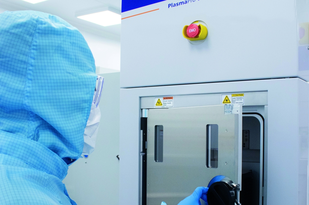
Back in September 2022 at the International Conference for Silicon Carbide and Related Materials (ICSCRM), held in Davos, Oxford Instruments, launched Plasma Polish. Originally conceived as either a replacement or a complementary process to a chemical mechanical polish (CMP), this alternative plasma-based process has been attracting significant interest from leading substrate manufacturers and vertically integrated device manufacturers. Wafers that have undergone Plasma Polish during processing into diodes and MOSFETs have a performance that’s in line with industry standard CMP, according to full wafer electrical measurements and yield results (see Figure 1).
The non-contact, dry Plasma Polish process has several key benefits including lower cost, a reduced environmental impact and the ability to remove subsurface damage.
Plasma Polish requires low levels of consumables and creates no toxic slurry, leading to an operating cost reduction of up to 85 percent, resulting from the removal of these process requirements and their associated costs. The absence of the slurry also means that there are no disposal issues and removes the significant water use typically associated with CMP, making Plasma Polish better for the environment. Plasma Polish uses industry standard non-toxic process gasses, making it unproblematic to install in production facilities.
The third benefit, subsurface damage removal, is unique to Plasma Polish. This great strength, discussed further below, comes without having to make any changes to either upstream or subsequent processes.

Figure 1. Plasma Polish achieves a high yield on full-wafer device tests.
Assessing crystal quality
We originally conceived of Plasma Polish as a technique for preparing SiC substrates for the subsequent growth of epitaxial layers. However, following significant market engagement, including demonstrations on customer material, more and more opportunities are emerging where Plasma Polish provides a solution to surface and subsurface damage.
At this year’s ICSCRM, held in Sorrento, Italy, we presented data that confirms that Plasma Polish removes subsurface damage. To prove this is the case, we developed breakthrough characterisation techniques by harnessing expertise from many parts of our business. Our validation of the subsurface damage removal capabilities of Plasma Polish comes from three metrology and crystal analysis techniques: contact-resonance atomic force microscopy; electron back-scatter diffraction, which is an electron microscopy-based analytical tool; and Raman microscopy.
Before setting out into the insights provided by these techniques, we’ll briefly explain how and why Plasma Polish works. It’s a technique that employs physical and chemical mechanisms able to access and remove subsurface damage, with the extent of this benefit dependent on the chamber design, its configuration and the process recipe. Wafers are processed in a reactor chamber on a radio-frequency-biased wafer stage at a low pressure – this enables the acceleration of the chemically reactive plasma gas onto the wafer surface. As any damaged or defective crystal is inherently weakly bonded, this unique form of plasma etch removes poor-quality material far faster than good-quality, strongly bonded crystal. Consequently, all that remains after a Plasma Polish is higher quality material exhibiting excellent crystallography. In stark contrast, while CMP provides planarisation (flattening), it fails to remove damaged material at a higher rate than good-quality crystal.

alpha300 Raman microscope for characterising chemical composition,
crystallinity, defects, strain, and doping in wafers up to 300 mm
To assess the crystal quality of SiC processed by Plasma Polish, we have turned to a variant of atomic force microscopy known as contact resonance. With this technique, we have mapped the sample surface with a cantilevered stylus that spot-measures the resonant frequency. From this it is possible to obtain a measure of crystal quality as a function of material stiffness, with sharper peaks at higher frequencies equating to higher quality.
We have used contact-resonance atomic force microscopy to compare the crystal quality of incoming unprocessed material and that processed by Plasma Polish. Incoming unprocessed material has a very broad peak at the lowest average frequency, indicating neither good crystal quality nor homogeneity (see the red curve in Figure 2).
To compare SiC processed by CMP and Plasma Polish, we performed four measurements on each wafer: one treated with CMP (Blue), and one treated with Plasma Polish (green). As the blue peaks are narrower than the red, we have concluded that CMP produces an improvement in quality compared with the incoming substrate. However, the four blue peaks are at markedly different frequencies, indicating variation. Meanwhile, the four narrow green peaks have significant overlap, indicating that Plasma Polish improves crystal quality and homogeneity.
The second technique that we have employed, electron back-scatter diffraction, characterises crystallinity and type at a depth of up to a few tens of nanometres. With this form of diffraction, we have produced two images of interest: a Kikuchi pattern at each imaged pixel; and a pattern quality map, revealing the quality of the pattern at each pixel.
For Kikuchi patterns, quality is defined by the sharpness of the diffraction pattern. If it is sharp, this indicates high crystal structure conformality; and if it is diffuse or blurry, it is evidence of either poor structure conformality or more than one SiC polytype. When electron back-scatter diffraction is used, a featureless pattern quality map with a bright colour indicates a high-quality, uniform surface.

Figure 2. Contact-resonance atomic force microscopy of four unprocessed
points of a CMP substrate (blue) and four points of a Plasma Polished
substrate (green).
When using a scanning electron microscope (SEM) to scrutinise pre-etch samples and those having undergone Plasma Polish, we obtained images that are actually very comparable, mostly showing topography (see Figure 3). This indicates that metrology techniques with more structural specificity are needed to offer greater insight into what is happening at the subsurface. Electron back-scatter diffraction meets this requirement, providing a true assessment of subsurface crystal conformality and polytype purity. Using this technique to study a pre-etched sample yields a pattern quality map with dark lines associated with damaged or amorphous crystal. Once Plasma Polish is applied, electron back-scatter diffraction creates a featureless pattern quality map, indicating improved crystal conformality and purity. The Kikuchi pattern is sharper and of higher quality, thanks to removal of damaged material by Plasma Polish.
Raman microscopy is the third and final SiC substrate characterisation technique we have utilised to assess crystal quality. This form of microscopy, which is incredibly sensitive to local chemical bonds, can penetrate to around 2 mm, thereby enabling the gathering of information from deeper in the crystal. By comparing specific Raman peaks in a spectrum, we are able to assess types of order and disorder. This is accomplished by determining an intensity ratio for two peaks: one peak corresponding to the 4H polytype of SiC, and the other corresponding to disordered Si-C.
We have produced histograms of measured peak ratios after acquiring Raman spectra across a whole SiC wafer (see Figure 4, which has red and green bars for measurements of unetched and Plasma Polish wafers, respectively). The green peak is narrower than its red counterpart and it is closer to the ideal ratio of zero. Based on these observations, we can conclude that Plasma Polish results in a superior crystal uniformity and a higher concentration of 4H SiC, the critical polytype for device production.

Figure 3. Electron back scatter diffraction (EBSD) images of pre-Plasma Polish and post-Plasma Polish Etch.
Additional opportunities
As well as replacing CMP, Plasma Polish can work alongside while offering a drastically lower operating cost, no toxic consumable usage or disposal, and a proven capability to remove subsurface damage and increase crystal quality. So, given all these great attributes, how can this advanced solution to preparing SiC substrates for epitaxial growth move forward? Well, there are limitless applications for dry Plasma Polish, where a traditional wet polish process is either not possible, or at least suboptimal. For example, Plasma Polish can rectify substrate bow/warp, optimise device process integration by swapping out wet cleans for dry polishes, reclaim substrates, maintain crystal quality on thicker epilayers for high-voltage devices, improve repeatability with integrated automatic endpoint process control and enable thinner substrates – note that all these opportunities apply equally for 150 mm and 200 mm material, thanks to the innate scalability of our process.
