Giving gallium oxide avalanche capability
Pairing Ga2O3 with NiO produces robust power electronics for harsh environments.
BY FENGZHOU AND JIANDONG YE FROM NANJING UNIVERSITY AND YUHAO ZHANG FROM VIRGINIA TECH
Advanced power devices are essential building blocks for high-efficiency energy conversion in a number of applications, including electric vehicles, data centers, electric grids and renewable energy processing. To reach higher levels of performance with these devices, the ultimate driving force is the selection of the semiconductor material. The last decade has witnessed the success of wide bandgap semiconductors, such as GaN and SiC. Compared to silicon, these alternatives have raised the bar. But even more impressive devices are now on the horizon, drawing on the superior strengths of ultrawide bandgap semiconductors, such as Ga2O3, diamond and AlN.
Regardless of the material used, the primary function of the power device is to operate as a switch between a high blocking voltage and a high conduction current. Due to this requirement, the ability to handle overvoltage and overcurrent events is indispensable for any power device. Armed with that attribute, power devices can temporarily survive common faults in power systems – they could be short circuits, excessive loads, or arc/ground faults – before protection circuitry intervenes.
Traditionally, avalanche and surge current capabilities have been realised with homogenous p-n junctions. However, this architecture has proven elusive in power devices based on ultrawide bandgap semiconductors, because it is incredibly challenging to realise bipolar doping, a requirement for making homogenous junctions.
One way to tackle this challenge is turn to the hetero-integration of foreign p-type oxides, such as NiO, which can be paired with n-type Ga2O3. It’s an approach that has been adopted by those of us at Nanjing University. Back in 2020, we broke new ground with the first double-layered p-NiO/n-Ga2O3 heterojunction power rectifier. It’s an innovation that enhanced the reverse blocking capability up to 1.86 kV and ensured stable operation at temperatures as high as 440 K. We then built on that success, producing β-Ga2O3-based bipolar power devices that combine a high current output with a fast reverse recovery and nanosecond switching. It’s a foundation that has put us in a great position to address the most critical avalanche and surge robustness challenges in Ga2O3 devices.
For that most recent challenge, we have joined forces with Yuhao Zhang’s team at Virginia Tech. It’s a collaboration that has borne much fruit, realising an exceptional level of avalanche and surge current robustness in NiO/Ga2O3 p-n heterojunctions through innovative device design and circuit evaluations.

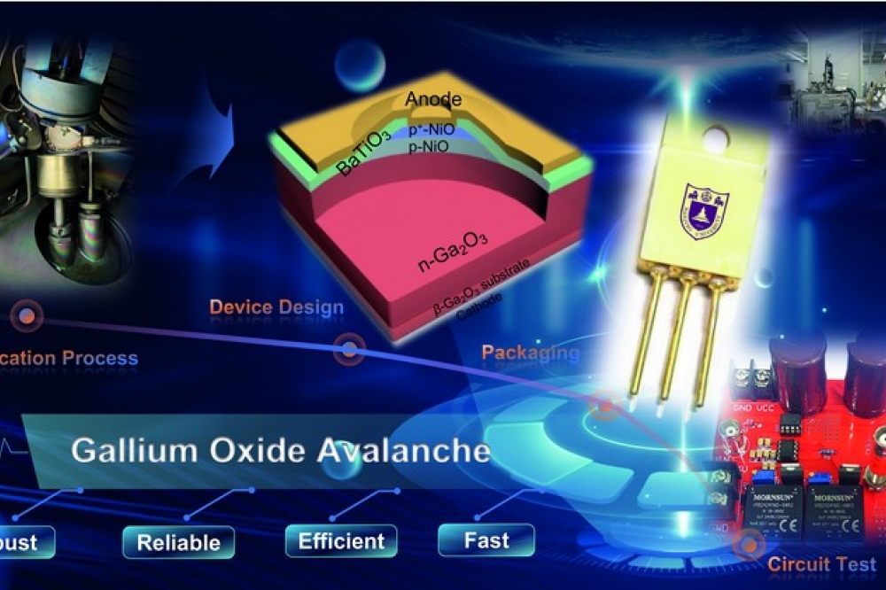
Figure 1. (a) Three-dimensional illustration of a fabricated NiO/Ga2O3
hetero-junction diode. (b) Simulated in-plane electric-field contour of
devices with the BaTiO3 dielectric layer. (c) Temperature-dependent
reverse current-voltage characteristics of the hetero-junction diode.
(d) Typical temperature-dependent unclamped inductive switching voltage
and current waveforms for Ga2O3 hetero-junction diodes at an inductance
of 1mH. (e) Surge current-voltage locus of the hetero-junction diode and
the reference Ga2O3 Sckottky barrier diode. (f) Reverse recovery
characteristics of the Ga2O3 hetero-junction diode, the reference Ga2O3
Sckottky barrier diode, and a commercial silicon fast-recovery diode.
Architectures for avalanche
For power devices, it is crucial to manage electric field crowding and prevent premature breakdown. Working together, our partnership has addressed this matter by developing an etching-free edge termination technology, featuring a small-angle bevelled double-layered NiO junction termination extension (see Figure 1 (a)). We use an amorphous BaTiO3 layer with an ultra-high dielectric to conformally cover the NiO junction termination extension structure in a consistent manner. Introducing this ultra-high dielectric ensures a nearly uniform electric field at the NiO/Ga2O3 junction, and ultimately enables a uniform and robust avalanche (see Figure 1 (b)). For circuit tests, we house a large-area (3 mm by 3 mm) NiO/Ga2O3 p-n heterojunction device in a TO-220 package.
Power devices with avalanche capability can withstand overvoltage stresses. Such devices are able to accommodate high avalanche current at the avalanche breakdown voltage, and dissipate excessive energy in circuits. The proven capability of our NiO/Ga2O3 heterojunction devices comes from rigorous testing, using both quasi-static current-voltage sweeps and dynamic unclamped inductive-switching circuit tests. These investigations reveal that the avalanche breakdown voltage increases with temperature (see Figure 1 (c)), with a positive temperature coefficient of 1 V/ °C – that’s a typical manifestation of device avalanche. According to unclamped inductive-switching circuit testing, our device produces textbook-like avalanche waveforms (see Figure 1 (d)). What’s more, the temperature coefficient of the avalanche breakdown voltage extracted from unclamped inductive-switching waveforms is identical to that extracted from current-voltage characteristics.
We have provided additional validation of our device’s robust avalanche capacity with 1 million cycles of repetitive avalanche tests. This confirms that compared with traditional homogenous p-n junctions, our ultra-wide bandgap heterojunctions offer superior performance and robustness for power applications.

Figure 2. (a) Illustration of the band diagram and carrier transport
dynamics under the avalanche condition. (b) Simulated profiles of the
electron and hole concentration, electric field and generation rate in
the hetero-junction diode under two different hole mobilities, at an
avalanche current of 30 A. (c) Electron-beam-induced current profile of a
NiO/Ga2O3 heterojunction to determine the minority carrier diffusion
lengths. (d) Illustration of the carrier transport dynamics under the
high forward current. (e) Simulated distribution of minority carriers on
both sides of the hetero-junction diode at a forward voltage of 6 V.
In addition to this avalanche capability, our NiO/Ga2O3 heterojunction demonstrates exceptional surge current capability, withstanding over 50 A of surge current. In stark contrast to the Schottky barrier diode, the surge current waveforms of our heterojunction device exhibit an anticlockwise locus signature, which signifies negative temperature coefficients for the differential on-resistance (see Figure 1 (e)). Surprisingly, the 1200 V reverse recovery time of our heterojunction device is at the nanosecond level (Figure 1 (f)) – that’s similar to the unipolar Ga2O3 Schottky barrier diode, and far faster than the bipolar silicon fast-recovery diode. Based on these results, it appears that our NiO/Ga2O3 heterojunction can deliver a simultaneous reduction in conduction loss and switching loss, compared with conventional bipolar devices.
Operating under extreme conditions
Thanks to our breakthroughs in avalanche and surge operation, we have been able to delve into the details of fundamental carrier dynamics in these ultra-wide bandgap semiconductor heterojunctions under extreme conditions. This includes high electric fields, high current densities, high temperatures, and non-equilibrium dynamic conditions.
The realisation of avalanche behaviour hinges on impact ionisation and multiplication occurring at the junction, as well as the efficient removal of non-equilibrium carriers that result from impact ionisation. As illustrated in Figure 2 (a), once impact ionisation is initiated in the n-type Ga2O3 drift layer, the strong electric field sweeps electrons and holes produced by this interaction to the cathode and heterojunction, respectively. Due to the staggered band structure, the NiO/Ga2O3 heterojunction produces no barriers to hole transport.
We have simulated the behaviour of our devices. These calculations suggest that holes produced by impact ionisation in Ga2O3 are exempt from controversial self-trapping, and drift with considerable mobility – it is this that enables a high avalanche current. The dynamic avalanche characteristics also allow us to extract a full set of electron and hole impact ionisation coefficients in Ga2O3, which is important for developing solar-blind avalanche photodetectors that could serve in numerous applications.
Yet another advantage of the robust surge capability of the NiO/Ga2O3 heterojunction is that it sheds new light on minority carrier (hole) transport in Ga2O3, which remains controversial and largely unexplored. Our efforts on this front, in partnership with researchers at the Australian National University, have involved imaging the minority carrier dynamics in NiO/Ga2O3 heterojunction diodes with a microscopic electron-beam-induced current (see Figure 2 (c)). This technique unveiled asymmetric minority carrier lifetimes for electrons in p-NiO and holes in Ga2O3 of 124.0 ns and 6.2 ns, respectively. Based on these values, we expect bipolar conductivity modulation to occur predominantly in NiO at high forward bias, primarily through electron tunnelling injection (this is illustrated in Figure 2 (d) and 2 (e)). When this device is being switched off, depletion mainly occurs in the lightly-doped Ga2O3. As minimal minority carriers need to be recombined in p-NiO for switching to occur, this has an insignificant impact on device reverse recovery.

Figure 3. (a) Electric field at avalanche versus avalance blocking
voltage benchmark and (b) surge energy versus reverse recovery time
(trr) benchmark, all for reported Ga2O3, GaN, SiC, and silicon power
diodes.
Benchmarking
Our NiO/Ga2O3 heterojunction sets new performance benchmarks by combining low on-resistance with high current capacity and a high blocking voltage. As summarised in Figure 3 (a), surge current and surge energy capacities surpass those of silicon devices, and are comparable to the best reported performances for SiC and GaN devices. It’s important to note that our heterojunction overcomes the fundamental trade-off between robustness and switching speed in conventional homojunctions (see Figure 3 (b)), clearing a path to advancing ultra-wide bandgap devices in power applications.
As well as the opportunities in power electronics, our innovative ultra-wide bandgap heterojunction architecture that features avalanche ruggedness has great potential for realising ultra-low noise avalanche photodetectors in the deep-ultraviolet spectral range. Such devices are expected to break through the fundamental trade-off between responsivity and response speed, a triumph that promises to have far-reaching implications in the fields of optoelectronics and photonics.
Further reading
H. Gong et al. “A 1.86-kV double-layered NiO/β-Ga2O3 vertical p-n heterojunction diode,” Appl. Phys. Lett. 117 022104 (2020)
F. Zhou et al. “1.95-kV Beveled-Mesa NiO/β-Ga2O3 Heterojunction Diode With 98.5% Conversion Efficiency and Over Million-Times Overvoltage Ruggedness,” IEEE Trans. Power Electron. 37 1223 (2022)
Y. Qin et al. “Recent progress of Ga2O3 power technology: large-area devices, packaging and applications,” Jpn. J. Appl. Phys. 62 SF0801 (2023)
F. Zhou et al. “An avalanche-and-surge robust ultrawide-bandgap heterojunction for power electronics,” Nat. Commun. 14 4459 (2023)
J. Kozak et al. “Stability, Reliability, and Robustness of GaN Power Devices: A Review,” IEEE Trans. Power Electron. 38 8442 (2023)