The road to SiC process control
Manufacturers of SiC power devices produce better transistors when
they turn to metrology techniques involving Fourier transform infrared
spectroscopy, optical critical dimension and picosecond ultrasonics.
BY NICK KELLER FROM ONTO INNOVATION
Efforts at curbing carbon dioxide emissions are stepping up, with more electric vehicles on our roads and the installation of renewable energy sources on the rise. Alongside these advances, the makers of these green technologies are increasing the electrical efficiency of their offerings, with silicon-based power devices being ditched in favour of superior alternatives based on the likes of SiC.
Supporting this move are the superior physical properties of these compounds. Compared with silicon, semiconductors such as SiC have wider-bandgaps, a higher electron saturation velocity, a higher critical electric field and a larger thermal conductivity. Drawing on all these strengths, power transistors offer higher operating frequencies, higher power ratings, elevated operating temperatures, better cooling capability and lower energy loss – just the traits that the market wants.
Today’s manufacturers of SiC power devices are tending to focus on trench-based devices, a design that reduces on-resistance and increases carrier mobility. But there is a trade-off, with these strengths coming at the expense of increased fabrication complexity.

Figure 1. SiC trench MOSFET process flow.
To address this issue, high-volume manufacturers of SiC power devices must adopt inline process control at several key steps, including optical metrology methods like Fourier transform infrared (FTIR) spectroscopy, optical critical dimension (OCD) and picosecond ultrasonics. When armed with these techniques, chipmakers are far better informed when undertaking critical processing steps, including epilayer growth, trench etch, gate poly-silicon etch back, and frontside/backside contact metallisation.
All of these three process control techniques that have just been mentioned can play a major role in streamlining SiC production. When FTIR is adopted alongside advanced algorithms, SiC manufacturers can extract epilayer thickness and carrier concentrations for two- and three-layer stacks. What’s more, FTIR can non-destructively characterise the depth and the dopants in the implant layer directly on SiC substrates before and after the anneal process step. That’s a significant benefit, as it removes the need for monitoring silicon wafers and secondary ion mass spectrometry when undertaking implant characterisation. Meanwhile, the introduction of a multi-channel OCD tool in a SiC fab can accurately and non-destructively determine trench depth, bottom and top widths, and bottom rounding at the trench etch step, when this technique draws on electromagnetic solvers that utilise advanced rigorous coupled wave analysis. Note that bottom rounding of the trench is critical to preventing a high electric field density, and ultimately premature device failure. Lastly, picosecond ultrasonics can improve efficiency in a SiC fab by measuring frontside and backside metal contact thickness. Together, these non-destructive, in-line process control methods empower chipmakers to solve many of the challenges posed by the increased fabrication complexity of SiC power devices.

Figure 2. PD Epi model fitted to the experimental spectra from the FTIR
system and the wafer maps for all parameters of interest.
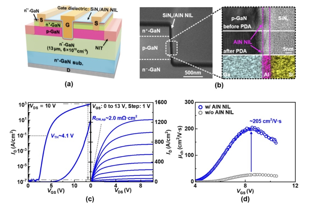
Soon we will take a closer look at all three techniques. But before we do, let’s take a minute to review the process steps for making a simplified SiC trench MOSFET and a SiC trench insulated-gate bipolar transistor (IGBT). This is outlined in Figure 1, which illustrates the process flow for the SiC trench MOSFET, and shows the key process steps, key parameters, device performance impact and the proposed process control solution. This figure also illustrates the process flow for a SiC trench IGBT device. While the steps are very similar, there are differences. The most significant is that a SiC trench IGBT has a p+ substrate and a n+ buffer layer before the drift layer.
Scrutinising layers with FTIR
Incorporating a Michaelson interferometer, a broadband light source and a fast Fourier transform (FFT) algorithm, FTIR spectrometers are well suited to studying the layers of SiC devices. This technique, requiring acquisition of infrared spectra extending from the near-IR to the far-IR, is quick, non-destructive and highly sensitive to molecular and free-carrier absorption. By measuring both transmission and reflectance spectra, a single tool can measure the elemental composition of epilayers and their thickness. A well-designed system is capable of obtaining the characteristics of five epitaxial layers from a single scan.

Figure 3. SRIM simulations for energy and dose skews, then raw FTIR
spectral response to those skews and finally correlation of FTIR
measurements to SRIM.
Spectroscopy in the IR offers much insight, including values for the carrier concentration of doped semiconductors. This is possible due to free carrier absorption, a process described by the Drude model, which accounts for the frequency-dependent conductivity of metals. The Drude model can be used to calculate the plasma frequency, which depends on the concentration of free carriers and their effective mass. For wavelengths above the plasma frequency, the electric field of the incident light oscillates so fast that the material acts like a dielectric. That’s not the case for wavelengths below the plasma frequency, which absorb light. Note that the absorption coefficient is directly proportional to the free carrier concentration.
The information garnered by FTIR spectroscopy is incredibly valuable to makers of SiC trench MOSFETs and IGBTs. For the SiC MOSFETs, the thickness and the carrier concentration of the drift layer directly determines the breakdown voltage of the transistor. Meanwhile, for the IGBT, the buffer layer thickness and the free carrier concentration determine a number of key characteristics, including switching speed and conduction losses.
FTIR spectroscopy also offers great insight into the ion implantation process. Measuring the depth and free-carrier concentration of the p, p+ and n+ regions is critical, because all these features influence the channel mobility, contact resistance, threshold voltage and saturation current.
At Onto Innovation we are supporting this task, having developed a new analysis engine called PD Epi, which enables the modelling of complex epitaxial film stacks in compound semiconductors. Our analysis engine provides direct modelling of carrier concentrations and film thicknesses of multiple layers, including the substrate. Utilising Drude oscillator models and gradient layers, our engines determine the carrier concentration profile through the structure during the diffusion and implantation process.

Figure 4. The spectral variation of the spectroscopic ellipsometry and normal incidence reflectometry OCD channels.
To illustrate the power of our PD Epi model, we have used it to characterise an IGBT epiwafer. Using our model we have determined the buffer and drift layer thickness, and the carrier concentration for the buffer layer and the substrate. This study involved a Design Of Experiment (DOE) methodology, with the drift layer thickness varied from 5 µm to 30 µm. while all other parameters of interest were kept constant.
An example of results on these IGBT epiwafers, obtained with our PD Epi model and fitted to the experimental spectra from the FTIR, is shown in Figure 2, which has wafer maps for all parameters of interest. We have correlated the measured drift layer thickness to the expected thickness. This gave a coefficient of determination (R2) exceeding 0.99, demonstrating that the predictive capabilities of the PD Epi model are accurate. The measured precision levels – that is, the standard deviation of repeat measurements – averaged 0.2 percent for the drift layer thickness, and 8.5 percent and 2.5 percent for the buffer free-carrier concentration and substrate free-carrier concentration, respectively.
Additional capabilities of FTIR spectroscopy are measuring the implant depth of aluminium ions, and detecting dose variations of this species after the ion implantation process and prior to annealing. Normally, dopants must be activated, so that FTIR can detect the effects. However, with our PD Epi model, manufacturers can conduct their measurements prior to dopant activation.

Figure 5. The physical model and the model fit to the experimental structure on the four DOE wafers.
To demonstrate this, we have used FTIR spectroscopy to measure dose and energy skews. This involved simulating the stopping range of ions in matter – allowing us to then model implant depth and carrier concentrations. Using this model as a reference for our FTIR measurements, we then simulated the energy and dose skews (see Figure 3, which also shows the FTIR measurement response to the skews, and the correlation of the measurements to the SRIM simulations).
As part of this particular effort, we used a simple Drude oscillator model to determine the free-carrier concentration, while floating the thickness. The thickness results coming from this model were used to correlate peak implant depth; that correlation is roughly 0.96. Following this, we used the maximum reflectance to correlate to the dose. Again, we obtained excellent correlation.
Determining dimensions with OCD
OCD has been used in semiconductor manufacturing for over 20 years. During that time its application has shifted from top-down approaches, like critical dimension scanning electron microscopy (CD-SEM) and image-based microscopy, to OCD for dimensional metrology. Driving this move has been the need to measure re-entrant and vertically recessed structures, which are invisible to top-down metrologies. Today, OCD metrology is an indispensable part of the process control loop in high-volume manufacturing.

Figure 6. A comparison of simulations using spectral ellipsometry (SE), normal incidence (NI), and combined SE and NI.
In contemporary thin-film and OCD systems designed for the specialty market, spectroscopic ellipsometry provides the gold standard for thin-film measurements. This is employed alongside polarised spectroscopic reflectometry, which collects specular scattering spanning the deep ultraviolet to the near-infrared from periodic structures, both 2D and 3D, at oblique and normal incidence, respectively. Analysing this data with our proprietary Ai Diffract software, which is an electromagnetic solver based on advanced rigorous coupled wave analysis, allows us to extract detailed structural information. Process engineers can draw on this when running advanced process control.
There are several advantages of OCD over other approaches, such as atomic force microscopy, CD-SEM, and transmission electron microscopy. Merits of OCD are that it’s: non-destructive; measurements may take less than a second; it is highly precise, offering angstrom level repeatability; and it is data rich, with the capability to measure tens of parameters simultaneously in complex 3D structures. However, OCD also has a significant disadvantage: being an indirect method, it requires a model to interpret complex spectroscopic data. Due to this, OCD metrology is seen by some as inaccurate and subject to long setup times. But both these drawbacks can be avoided with a model-guided machine learning algorithm that synergizes physical modelling with machine learning.

Figure 7. Picoseco nd ultrasonics measurement principles. The decaying
thermal component is subtracted from the signal to get the blue curve.
During production of SiC trench MOSFETs, OCD can be used at the key process steps shown in Figure 1. Of particular interest are the post-trench etch measurements. The trench etch is a key step because trench parameters, like bottom width, bottom rounding, sidewall angle, depth and roughness, contribute to key performance attributes, such as breakdown voltage, on-resistance, channel mobility, and time-dependent gate oxide breakdown. Evaluating the quality of the etch is paramount, because this step is challenging, due to SiC being extremely hard, chemically stable, and having a low selectivity to SiO2 hard masks.
To demonstrate the benefits that analysis with our Ai Diffract software brings to OCD of SiC MOSFETs, we have undertaken a DOE, processing the trench etch step on four wafers. We began by varying the etch time to skew the trench depth, and then carrying out spectroscopic ellipsometry and normal incidence reflectometry measurements (see Figure 4). Using a physical model, we fitted the data, finding an excellent correlation between the average trench depth measured with the Ai Diffract model, and the expected depth based on DOE conditions (see Figure 5).

Figure 8. Forty-nine point maps of (a) Ti 1000 Å, (b) NiV 3000 Å, and (c) Ag 1500 Å.
Building on this investigation, we considered other key parameters in the model, such as the trench bottom width. It’s possible to also measure these parameters. However, how do we know whether OCD has sufficient sensitivity and discrimination? To answer this, we used uncertainty and sensitivity analysis to predict specific parameter measurements (see “Uncertainty and sensitivity analysis” for details).
Following that, we used a model with Process Of Record (POR) conditions and defined seven floating parameters: trench depth, trench bottom width, trench middle width (at variable depth), trench top width, sidewall roughness, bottom roughness, and a parameter to vary the depth location of the middle width. We simulated individual OCD channels, spectral ellipsometry and spectral reflectometry measurements, and both channels together (see Figure 6). Based on results of these simulations, we concluded that combining both channels together gives the benefits that normal-incidence channel has for trench depth and that the spectral ellipsometry channel has in sensitivity to bottom CD and top CD. It is clear that one can measure all the key parameters impacting device yield and performance at the trench etch step using OCD metrology, due to the low predicted parameter of uncertainty and the degree of correlation.

Figure 9. Repeatability performance.
Pursuing picosecond ultrasonics
The third of the three process control techniques that we are recommending for producers of SiC power electronic devices is picosecond ultrasonics, a pump-probe technique using ultrafast laser pulses, typically with a duration of 200 fs. This is a very well understood and documented technique that involves focusing a pump pulse to a tight spot on the device surface, leading to the generation of a sharp acoustic wave. The resulting traveling acoustic wave reflects off various interfaces, and when it returns to the surface it changes surface reflectivity, which is measured by the time-delayed probe (see Figure 7, which provides a plot of surface reflectivity as a function of the optical probe-pulse time delay).
Picosecond ultrasonics reveals a lot of information about the material, with raw data including contributions from electronic, thermal and acoustic components. The thickness of the material may be extracted from this acoustic signature using the arrival time of the echo, and the longitudinal speed of sound in the material. Other properties such as roughness, density and elastic modulus can be characterised, depending on the application.
To provide a more thorough materials characterisation, the set-up can be used for time-domain thermos-reflectance measurements. Thanks to recent improvements in hardware, the thickness and the thermomechanical properties of a material can be characterised with a single configuration. With this non-destructive technique, chipmakers can measure multi-layer metal films simultaneously, and discriminate individual layers of repeating metal. As mechanical and thermal properties can be obtained quickly on micrometre-scale regions, spatially mapping is possible.
Showcasing the power of this technique for SiC power device manufacturers, we have used it to obtain the ohmic contact and conduction metal layer thicknesses of source and drain contacts of a SiC trench MOSFET. These measurements are highly valued, because they have a direct impact on contact resistance. In addition, the metal thickness uniformity impacts device reliability, and the metal roughness contributes to its contact resistance, due to the presence of crystallographic defects, such as micropipes, stacking faults and basal plane dislocations, as well as damage from etching and polishing steps.
Thanks to the advantages of picosecond ultrasonics, it is rapidly replacing more traditional methods such as four-point probe methodology, a destructive technique that only offers indirect thickness information and cannot detect missing layers or misprocessed wafers. Using picosecond ultrasonics, makers of SiC power devices can have far greater metallisation process control, with monitoring that includes the contact barrier (Ti/TiN), trench metallisation (W-based contacts), and both frontside and backside metallisation (Ti/NiV/Ag) stacks.

Figure 10. Multi-layer metallization stack measurement.
To illustrate such capability, we have produced wafer uniformity maps of a multi-layer metal stack (Ti/NiV/Ag), shown in Figure 8. Using a spot size of just 8 µm by 10 µm and a rapid measurement time – it is less than 4 s per site – it is possible to characterise full wafer uniformity. Selected metal layer stacks are highlighted in Figure 9.
We also offer an example of measurements of repeating metals in a multi-layer stack, in this case Ti/Al/Ox/Ti/Al (see Figure 10). The raw data shows an excellent signal-to-noise ratio, with echoes from every layer clearly resolved. Note that competing techniques, such as X-ray metrology, cannot provide details of individual layers in such a stack, while measurements on blanket films are not representative of product performance. To assist those running SiC fabs, recipes can be set up to flag missing layers or detect misprocessing.
As mentioned previously, in addition to thickness, picosecond ultrasonics can monitor roughness, especially for thick films (hundreds of nanometres to the micron range). Roughness provides a qualitative indicator for monitoring a well-established process. Illustrating this capability are measurements from an aluminium film (see Figure 11).

Figure 11. The correlation of PULSE measurement to transmission electron microscopy (TEM) and atomic force microscopy (AFM).
The road ahead
There is no doubt that power devices based on wide bandgap materials, such as SiC, are the future of the power electronics industry. Thanks to their superior properties, enabling performance enhancements over silicon-based devices, sales are climbing fast. According to Yole Group, global revenue will reach $6 billion by 2027. Much of that will come from the automotive industry, with Yole forecasting SiC will represent approximate 80 percent of that market.
High yield, high-volume production of SiC power devices is far from trivial. There are challenges associated with process control, which is needed in many of the key steps in the fabrication process. Offering tremendous assistance are FTIR, OCD and picosecond ultrasonics metrology – all provide SiC power device manufacturers with options to address these obstacles. And once these obstacles are removed, the highway is largely clear for high-volume manufacturing of SiC power devices.
• The author of this feature would like to thank the following members of the Onto Innovation team for their contributions to this article: Priya Mukundhan, Aseem Srivastava, Zhuan Liu, Andy Antonelli, and Robert Fiordalice.