Banishing barriers to GaN adoption

With performance advantages of GaN established and the challenges of
driving GaN HEMTs overcome, now is the time to address the outstanding
concerns of designers, such as price, availability and reliability.
BY DENIS MARCON FROM INNOSCIENCE EUROPE
Its not that hard to spot the significant benefits that come from replacing silicon power devices with those made from GaN. Consider, for example, e-bike chargers, which are 75 percent smaller when they incorporate GaN, allowing them to fit in a backpack; or USB-PD laptop chargers, which are around one-third of the size of those incorporating silicon-based devices; or data centre DC/DC converters, where the introduction of GaN halves the size and delivers a substantial hike in efficiency.
There are many reasons behind the application advantages provided by GaN, which is now well known for enabling reductions in size and gains in efficiency. One significant asset of devices made from this wide bandgap semiconductor are their absence of reverse recovery current, facilitating simpler architectures. And there are additional benefits, including: GaN’s ability to function at a higher frequency than silicon, thereby permitting the deployment of smaller passives; the significantly lower specific on-resistance, allowing GaN devices to be much smaller; and a 10-times-better figure of merit, based on the product of the on-resistance and the gate charge, that leads to far higher efficiencies. As a result, GaN will continue to proliferate in all application areas, including consumer, industrial, automotive and renewables, with uptake increasing the performance of all power conversion systems while trimming size, boosting efficiency and cutting costs.
GaN: the compelling case
Today, the market for GaN is buoyant, thanks to the laying to rest of previous concerns. However, that hasn’t stopped some designers of power converters from harbouring doubts that are slowing the mass uptake of GaN. The reasons for this reluctance chiefly centre around price and high-volume availability, but there is also anxiety surrounding second-sourcing.
The smartphone market ably illustrates these points. Despite a slight fall in shipments, well over one billion units are still sold every year, encouraging suppliers of GaN power devices to get their products designed into phone handsets. But before this occurs, four obstacles must be overcome. First, there needs to be a clear advantage behind this move. In addition, the GaN device must replicate the very low gate leakage characteristic of silicon; sell at a competitive price; and be available in massive volumes, to sustain the billion smartphones sold per annum and to meet demand for a quick ramp, to match the 6-to-9 month cadence of new model introduction.
At Innoscience we tick all those boxes. But that’s not all. We are innovating, with products such as the market’s first bi-directional GaN. This technology, which we refer to as VGaN, delivers clear and compelling benefits. It enables a superior alternative to the conventional approach to blocking current in both directions, which is to use an over-voltage protection unit in a battery management system that features two back-to-back silicon MOSFETs. Thanks to our progress, this pair of transistors can be replaced with a single VGaN HEMT, delivering an alternative that’s 50 percent smaller and more efficient (see Figure 1).

Figure 1. One VGaN can replace two back-to-back silicon MOSFETs.
One of our breakthroughs has been to address concerns associated with the leakage current. Many designers are not used to having to consider this, because the oxide under the gate of a typical silicon device blocks leakage. The oxide layer is not present in GaN HEMTs, and the gate can be modelled as two back-to-back diodes (see Figure 2).

Figure 2. Optimisation reduces leakage to below 3 µA.
To reduce leakage, we have optimised the epitaxy, device architecture and processing. Thanks to advances on all these fronts leakage has plummeted by almost a factor of ten, falling to below 3 µA at 85 °C for the lifetime of the device. It’s a level of performance that’s welcomed by smartphone manufacturers, and one that ensures that VGaN HEMTs are suitable for use as the load switch within handsets.
This innovation illustrates that if a company is to be a leading GaN supplier, it must be an integrated device manufacturer. Fabless companies will struggle to innovate, because they do not have the inherent ability to optimise epitaxy, architecture and processing.
If you scrutinise price and availability, you’ll soon see why GaN has failed to establish its presence in the smartphone market, despite the growing desire of both customers and suppliers. For a 10 percent market penetration of the one billion phones sold in 2022, makers of GaN power devices would need to produce 100 million units a year. To manufacture this volume requires the processing of either 3,000 8-inch wafers per month, or 5,400 6-inch wafers per month. If for a moment we ignore the capabilities of Innoscience, the total global capacity of GaN is only 16,000 6-inch wafers per month, according to market analyst Yole Intelligence. Consequently, this single application would demand about a third of the world’s capacity!
It’s a markedly different state of affairs once our capacity is accounted for. We are the biggest integrated device manufacturer completely focused on GaN. By using 8-inch wafers, we can produce GaN devices cost-effectively in extremely large volumes. Our capacity continues to climb, and by 2025 we will be producing 70,000 8-inch wafers every month, dwarfing the combined production of all other manufacturers.
The reliability issue
Crucial to success is reliability. For huge companies, such as the smartphone maker Oppo, GaN could never be incorporated within the handset if reliability were in doubt.
We have demonstrated that our devices are strong in this regard. According to evaluations described by JEDEC and accelerated life tests, we have 10-parts-per-million device failure rates for the gate acceleration factor mode that exceed 20 years (see Figure 3). The equivalent figure for the drain is more than 10,000 years.
Another crucial factor is avalanche ruggedness, a vital characteristic for silicon power MOS devices. To evaluate this capability, engineers tend to perform an unclamped inductive switching test.
To carry this out, the test device is turned on, causing the inductor to charge at a linear rate. Once the drain current is high enough, the device is turned off, causing the inductor to dissipate its stored energy. This drives the device into breakdown. The avalanching capability of the test device permits the dissipation of the inductor current, therefore restricting any further increase in voltage. The test device remains in breakdown until total energy dissipation.
We translate the results of this test into values for the time-in-avalanche and the energy-in-avalanche that the device can support. If the power device does not have avalanche capability, it must offer a far higher breakdown voltage to allow complete energy discharge of the inductor. This is the case for our devices, where a high breakdown voltage fulfils the inductive switching rating. For our low-voltage devices, the breakdown voltage is more than double the device’s rating, ensuring that these products handle voltage spikes safely and successfully pass such critical tests.

Figure 3. Accelerated life tests highlight the reliability of low-voltage VGaN.
Data centres
Smart mobile devices are certainly not the only market for GaN. Of the other opportunities, data centres offer a huge and growing market that is exceptionally power-hungry. Here, efficiency is the number one priority. Even an increase in efficiency of just 0.1 percent provides considerable cost savings. The miniaturisation that GaN enables is also valued, with smaller power conversion systems freeing up more space for computing units. However, to secure sales, GaN suppliers must also offer a large and available product capacity, as well as low prices.
Beginning with the transition from AC to DC, Figure 4 outlines the power conversion phases within a data centre. A normal design at the primary side, incorporating power factor correction and a pair of inductors alongside a capacitor, typically deploys 650 V devices. Meanwhile, on the low-voltage side, it’s the norm to use 100 V and 30 V parts when getting down to point-of-load devices. Here, typically as many as 80 or more low-voltage power transistors are used for every implementation. All of these parts must be deliverable in volume and at the right price.

Figure 4. There is huge demand for GaN in power-hungry data centres.
The benefits of our devices are illustrated in a 600 W full-bridge, constructed using a pair of inductors and a capacitor. When built using four of our 3.2 mΩ 100 V GaN INN100W032A HEMTs, the resulting design is just a quarter of the size of that based on a silicon solution, while delivering a 0.6 percent gain in efficiency. This equates to a reduction in energy consumption of almost 10 percent, ensuring significant costs savings and lower CO2 emissions.
Integrated solutions
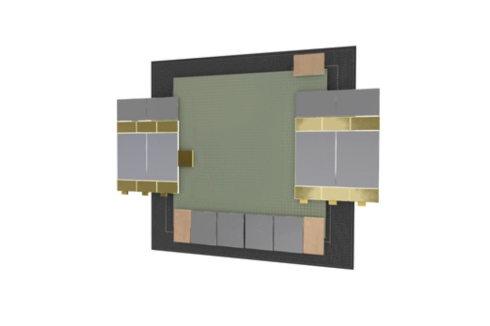
Further reductions in size are possible with integration. Consider, for example, our SolidGaN ISG3201, an entire half-bridge circuit that trims size by another 20 percent (see Figure 5). In this single-land-grid array package, measuring just 5 mm by 6.5 mm by 1.1 mm, there are two GaN HEMTs in half-bridge configuration, along with a driver and a bootstrap capacitor.
Note that the benefits of integration are not limited to scaling sizes. This approach also leads to higher performance, due to the package embedding connections between circuit elements. Consider once more the 600 W 48 V/12 V DC/DC converter for data centres. By introducing the ISG3201, designers can increase the power density and reach 1000 W in the same-size module at a heightened efficiency of 98.26 percent. This gives our customers the chance to choose between: a discrete solution, such as the INN100W032A, which offers greater flexibility; and an integrated solution, such as the ISG3201, which is easier to mount and use.
We have also directed our attention at the high-voltage sector with a portfolio of 650 V HEMTs with on-resistances ranging from 30 mΩ to 2.2 Ω. Again, we are aware that some designers will have concerns relating to avalanche failures due to high-voltage spikes. Once more, our approach to addressing this is to ensure headroom in the blocking voltage. Since GaN transistors – unlike those made from silicon – do not have an avalanche rating, the only way to avoid this form of failure is to select a device with a much larger breakdown voltage than the specified voltage rating. Our 650 V-rated devices can withstand non-repetitive pulses below 200 µs at up to 800 V, which is well above the maximum rating. When the duration of the repeat pulses shortens to below 100 ns, the maximum transient voltage our component can maintain falls to 750 V, both at room temperature and at 125 °C. This is still far beyond the 650 V rating, and adds to our collection of data that supports very reliable use.

Figure 5. Integrated SolidGaN solutions offer size, performance and ease-of-use benefits.
Dual sourcing
For very good reason, some of our customers are reluctant to rely on a single supplier. But they don’t have to, as multiple sources of GaN parts are emerging. For example, our 650 V/700 V devices in a DFN 8x8 or 5x6 package are pin-to-pin compatible with parts with a similar rating and specifications.
What’s clear is that there are no longer any barriers to GaN adoption in the mass power semiconductor market. Gone are the days when there would be concerns related to high-volume availability, price, compatibility between manufacturers, reliability at both low and high voltages, and avalanching. In short: the future is GaN.
Innoscience produces devices at its 8-inch fab in Suzhou, China.
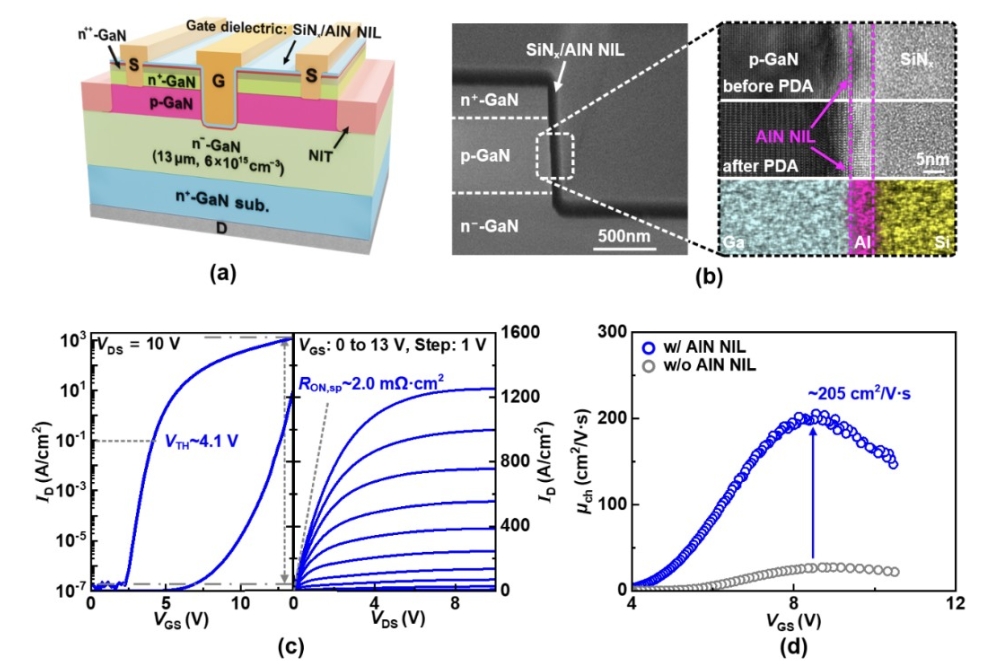
Reducing the on-resistance with a strain layer INNOSCIENCE’S GaN HEMTs are intrinsically enhancement-mode (E-mode) devices.
This much-preferred, fail-safe mode of operation, which is known as normally-off, is realised by growing a p-GaN layer on top of the AlGaN barrier, followed by the deposition and patterning of a gate metal and the selective recessing of the p-GaN layer over the AlGaN barrier. The gate metal layer forms a Schottky contact with the p-GaN layer and, as a consequence, the potential in the channel at the equilibrium is elevated to ensure normally-off operation.
By controlling all its manufacturing process stages in-house, Innoscience has been able to develop several technology improvements that have been key to optimising GaN HEMT manufacture for high performance and reliability, as well as mass production and cost reduction.
One of the critical parameters that determines transistor performance is RDS(on) – this is the total drain-source on-resistance per unit area. RDS(on) determines the maximum possible current rating of the switch and influences current loss, and thus efficiency. Consequently, by minimising the specific RDS(on), engineers can trim device size for a given on-resistance, and ultimately produce more parts per wafer, cutting costs.
To reduce specific RDS(on), Innoscience has developed a strain enhancement technology. A strain enhancement layer is deposited onto the wafer, immediately after the gate stack definition. Stress modulation created by this strain-enhancement layer induces additional piezoelectric polarisations; this causes the density of the two-dimensional electron gas to increase, leading to a fall in sheet resistance by 66 percent when compared with a device without the strain layer.
Crucially, since the strain enhancement layer is deposited after gate formation, it only affects the resistance in the access region. There is no impact to other device parameters, such as threshold and leakage. Thanks to this patented technology, Innoscience’s GaN-on-silicon E-mode HEMTs exhibit a very low specific on-resistance.