A new generation of physics-based tools steps into the WBG space

Wide band gap (WBG) semiconductors SiC and GaN promise a dramatic
increase in power performance. But these emerging technologies also
require new physics-based design tools to predict their performance and
help get the best out of them.
By Ahmed Nejim, R&D Collaborative Projects Director of Silvaco Europe
SiC and GaN chips pose many novel and different design challenges compared to silicon-based power devices. Issues such as bulk and interfacial traps, crystallographic stress, and anisotropic transport in 3D structures must be captured to provide the all-important insights required to add value and enable product differentiation.
Physics-based design software has been used in WBG power electronic R&D for decades. But as production ramps up to serve an increasing variety of commercial applications such as electric power trains and green energy, the search for improved device and circuit design is accelerating.
Stepping into this space are physics based numerical Technology Computer Aided Design (TCAD) automation tools.
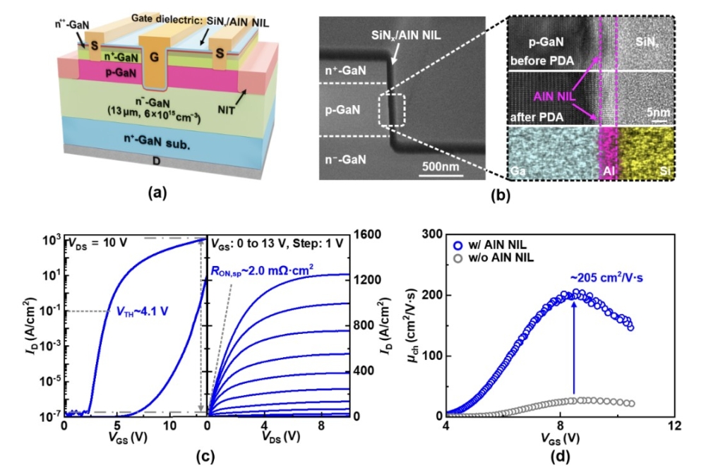
For decades, TCAD tools have enabled CMOS scaling and development along Moore’s law by capturing the manufacturing flow (process) and technology function (device) required for constant enhancement. Look at figure 1, which encapsulates the TCAD flow.

Figure 1. shows the fundamental concept of TCAD. Users define the structure usually through process simulation, then move to select charge carrier transport models to reflect the technology deployment conditions. Finally, the simulator produces device response and contours under different bias, temperature, frequency, and stress conditions.
WBG innovation starts with understanding the underlying material science and physical phenomena. This knowledge is then framed into numerical representation (models) that capture these phenomena. This is the stuff of long-term academic research and endeavour. While this is patently hard to achieve, the prize is the all-important insight into the technology performance beyond what can be measured in a lab. Look at figures 2a and b.

Figure. 2a shows electric field intensity contours in a SiC Junction barrier Schottky (JBS) diode under 1000V reverse bias. One can see the ‘attack’ of the field as it attempts to enter between the p-doped anode regions (shown as anode 2). Such insight and the location of the peak field helps designers optimise the distance between the regions and the doping profile to improve voltage blocking performance.

Figure. 2b shows the pGaN FET potential contours near breakdown. One can clearly see the role of the source shield plate in protecting the gate stack from the drain contact on the right. This helps designers in creating effective screening geometries.
Once these models are parameterised, a multidimensional design space is created. Such space is bound by the material parameters, manufacturing capability and required performance. From this space, the most valuable and lucrative products over the last 60 years of microelectronics have emerged to revolutonise our lives and economies and will do so again in the future. Automated design tools help discover these gems.
How is this done?
The process starts with intimate understanding of the semiconducting materials crystalline quality and its response to the manufacturing conditions (doping, oxidation, etching and thermal budget). In fact, everything that goes on in the fabrication line has to be captured here to develop a realistic representation of the technology.
Since WBG semiconductors involve grown stacks of diverse crystalline materials, the interplay between different crystalline structures must also be considered as it impacts charge transport. Although single crystals, these materials contain defects that play an active role in charge lifetime and recombination (traps). These traps reside within the bandgap and influence conduction under steady state and crucially under transient (switching) conditions. Knowing the concentration profile, energy level of these traps as well as their capture cross section will help produce realistic transient behaviours and current recovery plots. This is relevant for radio frequency (RF) applications as well as energy blocking switching performance. Furthermore, such defects might also contribute to leakage (tunnelling) currents which impacts device performance.
Since much of the transport events take place at material interfaces and heterojunctions, a clear representation of these must be captured. These include semiconductor-semiconductor interfaces which are key to WBG device stacks, dielectrics used in passivation and capping layers, and semiconductor metal contacts. The electrical contact material performance controls the leakage current and the final resistive path such as Drain Source on resistance (RDSon). Dielectric material quality plays a crucial role in managing the field distribution in the device and must therefore be modelled accurately. The next arena to enter is to model the charge carrier transport as a function of bias, geometry, stress, temperature and so on, to mimic device behaviour when placed inside circuits and products. Knowing how the technology would perform under product deployment conditions is the ultimate prize designers seek.
To give a flavour of the prominent issues facing WBG power electronics device designers contend with, here are few examples. In essence, designers need to track carriers from their generation (birth) to their recombination (death). Carrier lifetime, velocity and density is dealt with using various mobility models. These models respond to electric field strength and direction (field is a vector), temperature, carrier concentration, crystallographic orientation, and various scattering events.
Every so often carriers will encounter an energy barrier which blocks the usual drift diffusion transport while tunnelling probability through such barriers remains a possibility. This must be accounted for as key technology performance indicators are dependent on such events. Breakdown is calculated by considering carrier concentration amplification through internal impact rates under high electric field. Most of these phenomena are coupled so numerically robust tools are called for. As device geometry becomes more complex, 3D simulations become crucial. Look at figures 3a and b.

Figure. 3a shows breakdown in trench 4H-SiC power device. The impact ionisation rate distribution is shown along the wall of the trench as a function of trench slope and curvature in 3D. Vertical trench with sharp corners shows a hot spot while rounded and sloped trench shows a diffused distribution.

Figure. 3b shows the breakdown IdVd plots for the three configurations above. Red for the vertical sharp corner, green for the vertical rounded corner and blue for the sloped rounded geometry. Optimising the geometry in 3D space produces clear advantages in higher breakdown characteristics."
Consequently, these powerful tools have been used most effectively to develop power electronic products over the years and will play a crucial role in ramping up GaN and SiC based microelectronics. Technology issues such as voltage breakdown, leakage current and transconductance can be obtained readily from these calculations. However, since the interaction between the manufacturing conditions (fabrication flow) and device performance under steady state or switching conditions can also be quantified, and production yield can be better understood. This is especially important for mass market products such as automotive power trains and power management.
To improve the usage experience and reduce entry barrier, TCAD tools come with a wealth of models and material libraries that are based on many years of open literature and best practice, as well as the advanced graphical user interface (GUI) and data visualisation tools. Advanced meshing engines as well as multithreading calculations accelerate calculations and enable parallel (matrix) simulations rather than sequential ones. This improves productivity.
Other features such as open architecture that enable designers to customise their material parameters and transport models add value especially for novel technologies design such as WBG based power electronics.
Model robustness and the automation of these tools enable technology designers to investigate their design space made available to them by the manufacturability limits to best respond to market demands and differentiate from competitors. Such design of experiment (DOE) tools can quickly produce optimised compromise for the highest yield. The increased technology complexity represents a profound challenge in this area. The automation of these tools is an arena of significant R&D effort in recent years. The goal here is to add value with the smallest number of iterations and computational overhead.
Since design activities acquire greater commercial value as development moves from device to circuit then to system (increased abstraction level), a seamless link between device design and circuit (SPICE) design is of particular interest. Such simulation flow (Design Technology Co-Optimisation DTCO) establishes the link between manufacturing flow and device geometry on the one hand and circuit performance on the other. (figure 4) This will base circuit design on sound technology footings framed within the available manufacturing flows.

Figure. 4 shows the design tools in a design technology co-optimisation flow. The tools required to establish a seamless link between manufacturing and circuit simulation together with parasitic extraction and reduction.
Conclusions
TCAD tools especially when coupled with SPICE simulations within a DTCO flow propels WBG power electronics technology developments. They enable developers to discover the best available solutions for increased power efficiency, breakdown performance and high yield as well as product differentiation from competitors.
References
1) J.B. Casady et al, Status of silicon carbide as a wide-bandgap semiconductor for high-temperature applications: A review; Solid State Electronics Vol 39, Issue 10 (1996)
2) W.H. Lam et al, The Studies on Gallium Nitride-Based Materials; a Bibliometric Analysis. Materials (Basel); 2023 Jan 1;16(1):401
3) G. Giorgino et al, Study of Magnesium Activation Effect on Pinch-Off Voltage of Normally-Off p-GaN HEMTs for Power Applications; Crystals 2023, 13(9)
4) https://silvaco.com/tcad/