Unleashing GaN’s full ability for high-speed switching

GaN transistors can switch at much faster speeds than
silicon or SiC making them much more efficient. However, GaN transistors
can overheat if driven at more than 100 kHz, and generate unacceptable
levels of EMI.
Rob Gwynne, CEO of QPT Ltd, explains how his company has
solved these limitations to unleash GaN to work at up to 20 MHz and
deliver its full potential.
Operating GaN FETs at under 100 kHz means that their performance is similar to silicon or SiC, which limits the benefits to using GaN in the first place. As GaN transistors can transition from on to off at 1-2ns instead of 20-50ns for Si and SiC transistors, there is potential for a huge improvement in efficiency.
The core of the problem is that the expertise of power engineers is in the 10 to 100 kHz region where Si and SiC currently operate. Go above this and RF issues start to become a problem which requires solving them with a different set of skills, i.e., those of an RF engineer, with a Faraday cage to block the EMI. The second issue is the huge amount of energy within a tiny slice of GaN, which if not handled correctly means that the transistor will rapidly overheat.
This can be seen in figure 1 that shows the increasing amount of waste energy being produced as losses as the operational frequency of SiC and normal GaN increases. By contrast, the green line of GaN with QPT’s technology shows hardly any increase in energy loss.

Figure 1. Showing increasing losses as switching frequency increases
Why is there energy loss during the switching process?
A key application for GaN switching is to control an electric motor’s speed using a Variable Frequency Drive (VFD). For example, a three phase, 380V supply is changed into 540V DC (typically) using a Vienna rectifier. This DC is then chopped to provide the required frequencies to drive and control the motor. The higher the frequency, the faster the motor runs. Chopping means switching the DC bus on and off, making rectangular waveforms called Pulse Width Modulation or PWM.
As the width of these rectangular waves is varied, the power delivered increases or decreases. This digital on/off signal then either has to be averaged to a sine wave in a big external filter that is expensive and bulky. Or, in cheaper systems that don't have the filter, connected directly to the motor, where these high voltage, high speed transients degrade the bearings, the insulation and heat up the motor, wasting power and reducing the life of the motor.
In QPT’s approach, the high voltage PWM is filtered inside a VFD implemented with QPT modules using the company’s proprietary WhisperGaN construction system. Only pure sinewaves leave the module. Thus, no big, expensive, external filter is needed to generate sinewaves for the motor and the connected motor's lifespan is not degraded by this VFD. Energy is lost on the rise and fall of each transition from off to on or on to off. Shorten the time that this takes and less energy is lost.

Figure 2. Energy loss during switching
The smaller area under VDS/IDS curves results in lower power being dissipated (so faster switching results in less loss). This is dependent on the frequency that the controlling transistors operate at. To be precise, the majority of energy loss occurs when the transistor is neither on nor off. This energy loss takes the form of heat so that the transistor rapidly overheats, resulting in increased on resistance and, eventually, ceases to function.
GaN transistors are capable of switching in 1-2 ns, as opposed to 20-50ns for silicon and SiC transistors. Thus, GaNs are in this high energy loss region for almost no time at all and, consequently, they waste very little energy chopping the DC up into variable frequency AC to drive the motor at different speeds. This is the key to QPT being able to reduce energy wastage in a VFD by round 80 percent.
QPT’s technology
QPT has integrated its technology breakthroughs into two modules so that they can be easily implemented by customers with minimal effort and changes to existing designs. The qGaN module contains a 650V GaN transistor with the company’s qDrive that is the world’s fastest, most accurate, highest resolution, low jitter Isolated GaN Transistor Gate Drive. The second module is qSensor that combines the company’s ZEST and qSense technologies. It provides the sensing and control that enables the GaN to be driven at super high frequencies for the first time.
In addition, QPT has developed its WisperGaN construction system that includes a reference design for how the modules and the ancillary electronics can be assembled together in a Faraday cage so that there are no heating or RF issues.

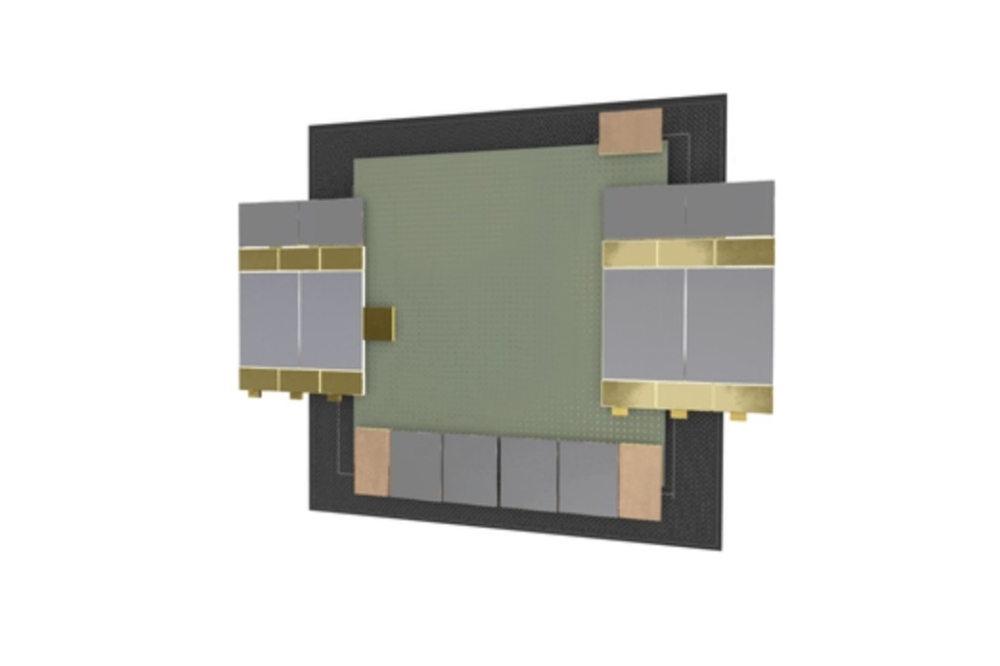
Figure 3. QPT's VFD modular design
The first qGaN module (Q650V15A-M01) will handle 15A RMS current driving 380V three phase motors. The roadmap will have qGaN modules to handle various different power loads to suit different application area requirements. Together with the other QPT technology modules, turnkey solutions can be easily assembled according to the reference design. The reference design is drop-in replacement for the power stage of existing VFDs without the need for any specialist expertise in EMC or thermal cooling.
The rest of the existing system such as the microprocessor and software stack stay the same. This makes upgrading a genuine plug and play solution with the benefits of needing less power so it effectively pays for itself in weeks.
In addition, there are further savings as the new BOM is less than existing solutions as it does not require external filters. Companies who want to upgrade from their current silicon solutions to be more power efficient can leapfrog over the hassle of developing a SiC solution in house and simply use QPT’s new GaN solution. 
Figure 4. Shows how typical VFD efficiency drops off dramatically and wastes energy as motor speed drops unlike with QPT technology
Variable frequency drives are not as efficient as currently claimed
VFDs work by chopping the incoming power to create a frequency that can be changed to adjust the speed of the motor. Energy is lost every time chopping occurs and, currently, VFD manufacturers believe this to be minimal hence their quoted 97 percent efficiency figure.
However, this figure is at full speed but, in reality, the speed varies and the efficiency drops significantly as the speed drops as shown in figure 2, which is what happens in a real-world operational cycle and is quietly ignored by manufacturers.
It is similar to car manufacturers only quoting fuel usage at the optimal speed and not mentioning the real-world figures of an urban cycle. It is important to note that in most applications, the motor speed is often down at the slow speeds so that the real-world efficiency drops significantly so that there is huge energy wastage that is currently being ignored.
QPT’s solution unlocks the ability of GaN to now operate at ultrahigh frequencies and deliver 99.7 percent efficiency at peak loads with hardly any decrease in efficiency at lower loads. This equates to up 80 percent reduction in VFD power usage compared to existing solutions that have to operate at much lower frequencies. This is shown as the green line on figure 2.
Combining the VFD power saving of around 80 percent with the motor usage gives around 10% reduction in overall power usage, which increases in applications where the motor is frequently at low speeds where the current solutions are inefficient.
Increasing the range of electric Vehicles
The efficiency of the motor controllers in Electric Vehicles can make a significant difference to their operational range. As explained, using QPT technology can reduce the power usage of the motor and VFD by around 10 percent or even more at low speeds which means either the vehicle goes further or that the battery can be made smaller for the same range.
An additional boost comes from integrating and shrinking the VFD. Current VFDs are bulky, which means that it is invariably located away from the motor itself and then connected by copper cables that are big and heavy to cope with the hundreds of Amps or so going through them. QPT’s next-generation GaN technology shrinks the size of a VFD to around a twentieth of the size, reducing weight, and, more importantly, the size reduction means that it can be co-located beside the motor.
This integrated motor solution eliminates the need for long heavy copper cables, which can total up to a significant weight and cost reduction at around half a meter each. Additionally, the copper cables have resistance creating power loss and reducing the overall system efficiency. All these factors mean that QPT’s solution without copper cables can increase the range of the car.
Reduce power wastage to help combat climate change
The company estimates that the high voltage, high power, hard switching, electric motors application markets where its new technology can be used to provide significant power savings is a Total Addressable Market of $365 billion that includes heat pumps, HVAC, EV and industrial motors. Currently electric motors account for 45 percent of global electricity usage and so by using QPT’s technology, they will be more efficient by around 10 percent and that means less carbon dioxide emissions which helps combat climate changes.