
GaN-on-silicon power devices start shipping
As sales of sales compound semiconductor devices other than LEDs look to pass $2 billion by 2020, SEMICON West adds a compound semiconductor technology program this year to look at volume manufacturing technology issues.
RF GaN, power SiC and power GaN devices should all see healthy double-digit growth, pushing each of these segments to more than $500M in sales by 2020, for a total compound semiconductor device market that will top $2 billion, according to Yole Développement. Though people have been talking about it for years, the GaN-on-silicon devices are just now finally starting to ship in qualification volumes, and will start to see real impact in a couple of years, says Philippe Roussel, leader of Yole's compound semiconductor business, who will speak at the SEMICON West 2014 program.
Although wide-bandgap compound semiconductor devices are already a $15 billion market, today that's almost entirely (>90 percent) for LEDs, and demand for LED lighting will soon start to level off, as the replacement lighting market saturates. But now that GaN-on-silicon suppliers have made good progress on controlling the bowing, cracks and dislocations from the lattice and thermal mismatch of growing the two materials, GaN power devices that outperform silicon at high voltages should at last soon begin to ship in volume.
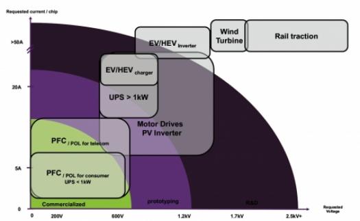
"Once the 600V GaN devices are available and qualified in volume, it will really open doors for markets from PV inverters to electric vehicles," says Roussel.
Who will make this GaN on silicon, however, is still up for grabs. Currently the makers of LEDs, laser diodes and power devices tend to deposit their own epitaxial GaN in house, as the ability to grow high quality film is a core advantage. But as the GaN-on-silicon technology matures to more of a commodity, some power device makers, and especially new entrants, may decide to buy GaN epi wafers from wafer or epi suppliers and do the front end processing in house themselves, instead of investing in MOCVD capacity.
Most of the major LED makers have been researching GaN-on-silicon as a cost-saving alternative to sapphire or SiC substrates, but the main advantage will accrue to those who can use existing depreciated 6-inch or 8-inch silicon fab capacity to significantly reduce costs. These LED makers could then also potentially use their depreciated surplus GaN epi capacity to enter the power device market, potentially reducing production costs by some 20 percent compared to suppliers without this depreciated capacity. It would, however, take them several years to develop the power technology, and distribution in the new market would be a challenge, notes Roussel.
GaN-on-silicon will impact GaAs RF devices in mobile front end as well
"The most interesting development for the future of high efficiency broadband is GaN on silicon," says Thomas Meier, TriQuint VP of Central Engineering, another speaker at SEMICON West.
In Meier's opinion, GaN's high voltage performance, high power density and high efficiency could well be the best solution for broadband power amplifiers needed for the proliferation of bands in high-end wireless application, if and when GaN-on-silicon brings the cost down.
Meanwhile, Meier expects GaAs to continue to dominate the power amplifier business for the mobile front end, but both silicon and GaN will likely see increasing share over time. He figures that over the next three to five years, GaN will likely move from high performance military and network applications into the mobile front end, replacing GaAs from the high end, as GaN-on-silicon technology now being developed for other applications matures.
Silicon will also likely take share from GaAs in the mobile front end in less expensive phones, but it will not take over the business, Meier argues, as GaAs will continue to offer the better RF performance that matters most at the high end. Silicon can be lower cost and can integrate controls on the same SOI die with the power amplifier, but those advantages could be limited. The very small power amplifier die is only a very minor part of the cost of the entire module of chips of multiple different technologies, from BAW filters to passives, that are most sensibly integrated at the package level, he suggests.
These speakers will be joined by Marina Sofas, technology manager of the new U.S. Dept. of Energy Wide-Band-Gap device manufacturing research program; Primit Parikh, president and co-founder of Transphorm; Sameer Penharkar, power device and wide-bandgap roadmap manager and Fellow at Texas Instruments; Frank Burkeen, VP & GM of KLA-Tencor's Candela division; and Klaus-Dieter Lang, director of Fraunhofer IZM,, in discussing what's needed to move emerging compound semiconductor devices to volume markets, at SEMICON West 2014 (www.semiconwest.org), July 8-10, in San Francisco. Issues of integrating compound semiconductors on silicon will also be covered in a separate silicon photonics program.


