
GaN on CMOS-compatible on-axis silicon (100) for hetero-integration
Maskless selective area epitaxy could result in large scale global adoption for GaN-on-silicon (100) power devices
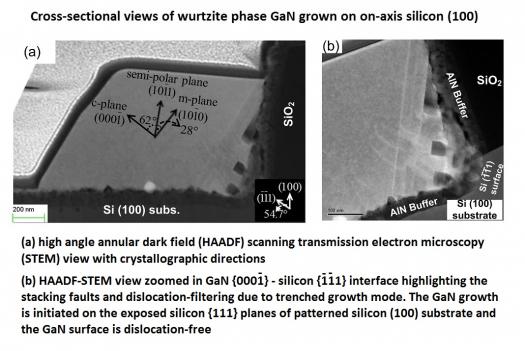
A new maskless selective epitaxy process of GaN on CMOS-compatible on-axis silicon(100) substrate is shown to have low dislocation density of less than 108 /cm2. Also, the GaN produced using this method is stress-free and has a low substrate wafer-bow; ideally-suited for GaN-silicon (100) hetero-integration.

SEM images of (left) conventional and (right) selective MOCVD growth processes on the same groove structures
Gallium Nitride (GaN) semiconductor technology is unique as GaN electronic devices (e.g. high electron mobility transistors) outperform existing ones (such as silicon and gallium arsenide) in high power and high frequency applications thanks to inherently high critical electric field (~ 3.5 MV/cm) and saturation velocity (~ 2.5 à— 107 cm/s).
However, without an environmentally friendly and cheap mass-production scheme, GaN semiconductor technology cannot be adopted on a large scale and such technological benefits will be limited to laboratory experiments and niche applications rather than world-wide adoption.
Recently, GaN-based electronic and photonic devices have drawn the attention of industry for high power/frequency and general lighting applications and driven the wide-scale metal-organic chemical vapour deposition (MOCVD) installation for GaN epitaxy. With such an infrastructure, it becomes essential to enable transitioning hetero-integrated devices benefiting from already-established silicon-based CMOS technology as well as reduce cost.

Broader growth demonstrations of selective GaN regrowth on silicon (100) substrate. This approach could be useful for interconnects as well as novel device architectures. The oxide pattern can be used to locate GaN layers along the periphery
Silicon (111) is an ideal substrate alternative to sapphire and silicon carbide (SiC) for GaN device production as it has almost a century long know-how, is inexpensive, and is available in large diameters. However, adoption of silicon (111) as the GaN substrate requires overcoming the material issues (lattice-mismatch (~ 17 percent) and thermal-mismatch (~ 53 percent)) between GaN and silicon (111) that conventionally lead to very high defect densities (~ 109 /cm2) and cracks.

Nonetheless, earlier efforts suffered from material issues (lattice-mismatch and thermal-mismatch) between gallium nitride and silicon that conventionally lead to very high defect densities (~ 109 /cm2) and cracks.
What's more, for true integration with silicon electronics, it is essential to develop GaN epitaxy on on-axis silicon(100) substrates as offcut in silicon degrades the CMOS performance (either n-MOS or p-MOS dependent on offcut direction).
In a recent study in the journal of Advanced Functional Materials, IBM Research shows that maskless selective area epitaxy, integrating low-defectivity (dislocation density) and stress-free GaN on CMOS-compatible on-axis silicon (100) substrates, could be the solution.
The performance of GaN devices is ultimately determined by the quality of the GaN. For many applications it would be ideal if one could achieve low dislocation densities (< 106 /cm2) and stress-free GaN over wafer-sized areas. However, no such material has been demonstrated on CMOS-compatible on-axis silicon (100).
For example, GaN on silicon (111) suffers from high dislocation densities (> 1011 /cm2) and wafer bow. Although the single-crystal GaN can be epitaxially grown on offcut on axis silicon (100) substrates, such substrates are not CMOS-compatible and GaN regrowth suffer from similar issues. This work, on the other hand, is compatible with conventional CMOS processes, and provide a novel roadmap for making GaN-based devices cost-competitive and co-integrated.
Some practical applications of this technology involves localised GaN devices. As the transistor technology is within tens of nanometres, it is indeed feasible to use such localised epitaxial high quality materials for GaN transistors - lateral or vertical stacked.
The work has been described in detail in the paper, "Cubic Phase GaN on Nano-grooved silicon (100) via Maskless Selective Area Epitaxy," by Can Bayram et al in Advanced Functional Materials, 2014.


