
Vishay launches asymmetric dual TrenchFET
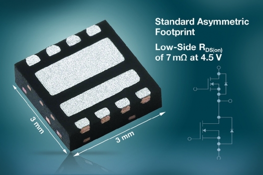
Vishay Intertechnology has introduced a new 30 V asymmetric dual TrenchFET power MOSFET in the PowerPAIR 3 mm by 3 mm package utilising TrenchFET Gen IV technology.
Providing 57 percent lower on-resistance, up to 25 percent higher power density, and 5 percent higher efficiency than previous-generation devices in this package size, the Vishay Siliconix SiZ340DT helps to save space and simplify the design of highly efficient synchronous buck converters by combining a high-side and low-side MOSFET in one compact package.
The TrenchFET Gen IV technology of the SiZ340DT utilises a very high-density design to reduce on-resistance without significantly increasing the gate charge, minimising conduction losses and reducing total power loss for higher power output.
As a result, the low-side Channel 2 MOSFET of the SiZ340DT offers a low on-resistance of 5.1 milliohms at a 10 V gate drive and 7.0 milliohms at 4.5 V. The high-side Channel 1 MOSFET features on-resistance of 9.5 milliohms at 10 V and 13.7 milliohms at 4.5 V.
The device is optimised for synchronous buck designs in 'cloud computing' infrastructures, servers, telecommunication equipment, and various client-side electronic devices and mobile computing applications.
The intended DC/DC blocks include system auxiliary power rails in servers, computers, notebook computers, graphic cards, gaming consoles, storage arrays, telecom equipment, DC/DC bricks, and POL converters. The SiZ340DT can also be used in DC/DC conversion circuitry that supplies power to FPGAs.
In these applications, the device maintains a low gate charge of 5.6 nC for the Channel 1 MOSFET and 10.1 nC for Channel 2. The resulting low on-resistance times gate charge - a key figure of merit (FOM) for MOSFETs in DC/DC converter applications - reduces conduction and switching losses to improve total system efficiency.
With higher efficiency, the SiZ340DT can run 30 percent cooler than previous generation devices at the same output load, or provide increased power density.
For typical DC/DC topologies with 10 A to 15 A output current and an output voltage below 2 V, the compact SiZ340DT saves up to 77 percent PCB space compared with using discrete solutions, such as a PowerPAK 1212-8 MOSFET for the high-side and a PowerPAK SO-8 for the low side.
Reducing switching losses, the device allows higher switching frequencies beyond 450 kHz to shrink the PCB size, without sacrificing efficiency, by enabling the use of smaller inductors and capacitors. In addition, by providing higher performance than multiple paralleled previous-generation devices, the MOSFET can potentially reduce the overall component count and simplify designs.
The SiZ340DT is100 percent Rg- and UIS-tested, halogen-free according to the JEDEC JS709A definition, and compliant to RoHS Directive 2011/65/EU.
Samples and production quantities of the SiZ340DT are available now, with lead times of fourteen to sixteen weeks for large orders.


