
News Article
Azzurro achieves "1 bin" wavelength GaN-on-Si LED wafer
While showing production values of less than 3 nm wavelength uniformity, Azzurro's 1.0 nm result came straight from development.
The 1.0 nm result demonstrates the capability to achieve "1 bin" GaN-on-silicon LED wafers with Azzurro's technology.
After questions about achieving competitive brightness and efficiency levels have been answered by various GaN-on-silicon contenders, the yield question has remained open. The large mismatch of crystal lattice structure and thermal expansion coefficient cause highly bowed LED wafers after and during growth.
This in turn has a very big negative impact on uniformity levels for wavelength, forward voltage and output power. Azzurro uses its proprietary and patented strain-engineering and growth technologies to overcome these obstacles.
Breakthrough uniformity from production for wavelength (less than 3 nm or 0.6 percent), forward voltage (1.3 percent) and output power (3.9 percent) for highly reduced binning were presented at the ICNS-10 in Washington D.C., USA together with excellent crystal quality values for 150 mm blue emission GaN-on-silicon LED wafers (all values are standard deviation).
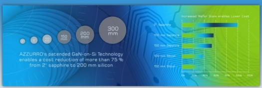
At the same time equally impressive values for 200 mm LED wafers show Azzurro's technological scalability. Manufacturability parameters like low bow (less than 20 µm) and thickness uniformities (1.7 percent) are not compromised on.
Based on these achievements the technical team continues to push for the ultimate "1 bin" wafer aim and demonstrated the benchmark result for wavelength with only 1.0 nm uniformity and a min/max value of 5 nm (one wavelength bin). This is illustrated in the map below.

Azzurro's latest results from production and development indicate that in addition to the cost advantages from lower cost substrates and by using standard silicon fabs for LED chip processing GaN-on-silicon LED wafers with the right strain-engineering technology can also help reduce binning dramatically.
The firm's co-founder and CMO, Alexander Loesing, who is also heading its LED Technologies business unit, comments on the results, "We are very proud of our team's record 1.0 nm achievement. With these results we show that our GaN-on-Si technology can bring the LED industry closer to the aim of making "1 bin" LED wafers."
Azzurro manufactures epitaxial wafers for LED and power semiconductor applications using silicon substrates.


