
X-FAB: making six inch SiC a reality
Can a Texas-based silicon wafer fab accelerate six inch SiC production? Compound Semiconductor talks to X-FAB Silicon Foundries to find out more.
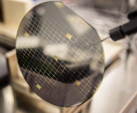
Image: X-FAB intends to drive the SiC industry's transition from four inch to six inch production.
Today, the vast majority of SiC diodes and transistors are fabricated on four inch wafers. But in a bid to increase device yield per substrate and cut production costs, SiC production is edging towards six inch wafers as the market grows.
One company, intent on pushing this transition forward is Germany-based X-Fab Silicon Foundries. Since 2013, the company has been busy adapting six-inch CMOS production at its Texas facility ready for SiC production, and earlier this month, deemed the plant 'SiC-ready'.
"[Back in 2013] all SiC manufacturing was on four inch wafers, but six inch wafers were becoming available and we could see that this transition would soon be underway," says Andy Wilson, Director of Strategic Business Development at X-Fab.
"We also wanted to leverage the economy of scales of our six inch CMOS manufacturing capacity," adds Wilson. "Converting our tools to run six inch, rather than four inch, SiC wafers was actually easier."
So X-FAB started the not-so-trivial process of six inch SiC wafer conversion. According to Wilson around 90% of SiC production processes could be supported by equipment already on X-FAB's CMOS line, while other tools needed to be adapted.
"For example, the thickness of a silicon carbide wafer is about half that of a silicon wafer, so steppers, coaters and deposition equipment needed some conversion," he says. "Also, the silicon wafer is opaque while the SiC wafer is translucent, so we made some significant changes to our [sensor-based] automated handling equipment."
The company spent the best part of 2014 developing what Wilson calls its 'hybrid' production, being able to switch capacity back and forth between CMOS and SiC manufacturing.
At the time, any SiC process steps that couldn't be accommodated by CMOS equipment, such as high temperature implantation and annealing, would be outsourced. And of course, subsequent SiC steps that could be carried out on the emerging integrated CMOS-SiC line would then be brought back in-house.
But come 2015, change was afoot. The US Department of Energy had launched its massive $146 million PowerAmerica Institute, uniting academia and industry in a mission to drive wide bandgap semiconductors costs down so as to be cost-competitive with silicon power electronics devices.
X-FAB joined the Institute, alongside the likes of Cree, Transphorm, Toshiba and United Silicon Carbide, and was tasked with providing the six inch wafer fabrication services necessary for device production.
And as part of the public-private partnership, the company received the all-important funds to invest in the specialised SiC processes it needed to run an entire six inch SiC production line, without outsourcing.
"Back in 2013 we were not in a position to justify the investments for these highly specialised SiC tools," points out Wilson. "But in early 2015, PowerAmerica provided matching funding which allowed us to buy the processes that are unique to SiC, several years earlier [than planned]."
Time to invest
Since 2015, X-FAB has secured a high-temperature anneal furnace, backgrind equipment for thinning SiC wafers, backside metal sputter and backside laser anneal tools.
What's more, a high temperature implanter is scheduled for installation later this year, and Wilson is now looking forward to seeing the foundry capitalise on its economies of scale.
The Texas facility can churn out up to 30,000 silicon wafers a month, and as the X-FAB director adds: "We can imagine that if we were running solely SiC discrete power devices, capacity would be even higher than 30,000 wafers a month."
Clearly X-FAB could bring unprecedented manufacturing scale to six inch SiC production, and, thanks to its existing CMOS processes, at an affordable cost.
"We can expand our SiC capacity as demand for device increases, while our silicon business will have absorbed the majority of the enormous fixed costs associated with expansion," says Wilson.
"With this cost structure and by keeping our overheads manageable, I feel we can really accelerate the commercialisation and adoption of SiC power devices," he adds.
So where next for X-FAB? Still part of PowerAmerica, the company will continue to provide SiC foundry services to Institute members but will now offer manufacturing capabilities to SiC device manufacturers worldwide.
"We purchase six inch SiC epiwafers and perform the necessary wafer processing required to create functional devices," says Wilson. "So we can supply to fabless vendors while device manufacturers could also add X-FAB as a second source supplier or use us as an alternative [manufacturer] as they move from four inch to six inch wafer fabrication."
To date, X-FAB has focused on fabricating SiC diodes and MOSFETs, as well as other switch architectures, for automotive markets, but fully intends to move into industrial markets. What's more, the company would also consider the manufacture of GaN-on-SiC devices for RF markets.
"X-FAB is bringing something different to the market," says Wilson. "The scale of our facility and our economies of scale are certainly unique in the foundry world, especially at six inches."


