German research cluster announces AlN success
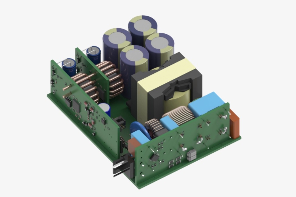
A new semiconductor technology based on AlN for power electronic transistors as well as mmWave radio-frequency circuits has the potential to significantly reduce losses in electrical energy conversion and high frequency transmission, according to German research partners.
Devices on single-crystal AlN wafers reach a higher power density and efficiency compared to GaN technology. They also show lower dynamic parasitic effects and a higher reliability. At the same time, the high thermal conductivity of AlN enables good heat dissipation of the devices.
In order to make AlN technology accessible to industry in the medium term, the related existing activities in Germany have been combined in a strategic cluster,.
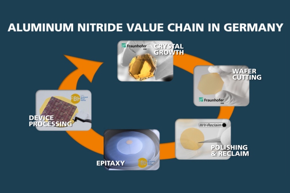
The aim is to establish a German value chain for AlN-based technology and to build up an international leadership position in this increasingly economically important field. The Ferdinand-Braun-Institut (FBH), the Fraunhofer Institute for Integrated Systems and Device Technology IISB and the company III/V-Reclaim PT GmbH drive this initiative together.
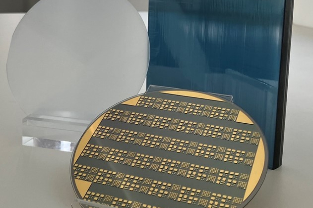
They cover the entire value chain, starting with the growth of AlN crystals using the Physical Vapor Transport (PVT) process, to wafering and polishing of epi-ready AlN-wafers, and the epitaxy of the functional device layers, up to the fabrication of transistors for power electronics and mmWave applications.
For the first time, the consortium has now successfully demonstrated the practical implementation of a value chain for AlN devices in Germany and Europe.
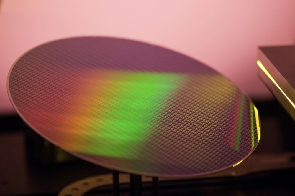
To this end, AlN crystals were grown at Fraunhofer IISB and sliced into AlN wafers with a diameter up to 1.5 inches. The company III/V-Reclaim has developed a polishing process for epitaxial wafer production. Functional epitaxial layers were then applied to these wafers at the Ferdinand-Braun-Institut, and AlN/GaN HEMTs were successfully processed on them.
The first transistor generations produced with these wafers already show promising electrical properties, such as a breakdown voltage of up to 2200 V and a power density superior to SiC as well as GaN-based power-switching devices.
Compared to established silicon devices, AlN/GaN HEMTs, as successfully produced on AlN wafers, offer up to three thousand times less conduction losses than with silicon and are around ten times more efficient than SiC transistors.
These research breakthroughs were supported by funding from the German Federal Ministry of Education and Research (BMBF) within the ForMikro-LeitBAN and Nitrides-4-6G projects.