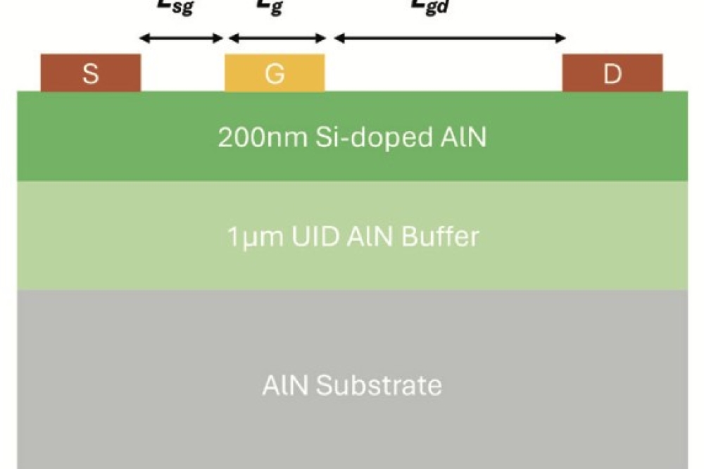
Infineon tackles GaN package standards
GaN suppliers have taken various approaches to packaging, leading to a lack of multiple footprint-compatible sources for customers. Infineon has addressed this challenge with its CoolGaN G3 transistor 100 V in RQFN 5x6 package (IGD015S10S1) and 80 V in RQFN 3.3x3.3 package (IGE033S08S1).
“The new devices are compatible with industry-standard silicon MOSFET packages, meeting customer demands for a standardised footprint, easier handling and faster-time-to-market,” said, Antoine Jalabert, product line head for mid-voltage GaN at Infineon.
The CoolGaN G3 100 V transistor devices will be available in a 5x6 RQFN package with a typical on-resistance of 1.1 mΩ. Additionally, the 80 V transistor in a 3.3x3.3 RQFN package has a typical resistance of 2.3 mΩ.
According to Infineon, this chip and package combination allows for high level of robustness in terms of thermal cycling, in addition to improved thermal conductivity, as heat is better distributed and dissipated due to the larger exposed surface area and higher copper density.
Samples of the GaN transistors IGE033S08S1 and IGD015S10S1 in RQFN packages will be available in April 2025.