A debut for the native AlN transistor
Researchers from Arizona State University are claiming to have fabricated the first AlN transistor that’s grown on a native substrate. The team’s metal-semiconductor FET (MESFET) has a breakdown voltage of more than 2 kV, alongside what’s said to be ‘decent’ values for drain saturation current and the on-off ratio.
Spokesman for the team, Houqiang Fu, told Compound Semiconductor that there are opportunities for AlN MESFETs in power electronics and RF electronics, due to the potential of these transistors to operate at high voltages, high breakdown fields and high-power densities.
AlN, a member of the family of ultra-wide bandgap semiconductors that includes Ga2O3 and diamond, boasts the highest bandgap of 6.2 eV and the highest breakdown electric field of 12 MV cm-1. It is these strengths have spurred interest in AlN devices, which need to overcome issues related to defects, doping and contacts. Examples of these challenges include an ionisation energy for silicon, the common n-type dopant, of more than 200 meV, and the tendency for metals to form Schottky-like contacts rather than ohmic ones.
The success of Fu and co-workers comes after reports from a number of groups of the fabrication of AlN Schottky barrier diodes on AlN substrates, and AlN MESFETs on foreign substrates.
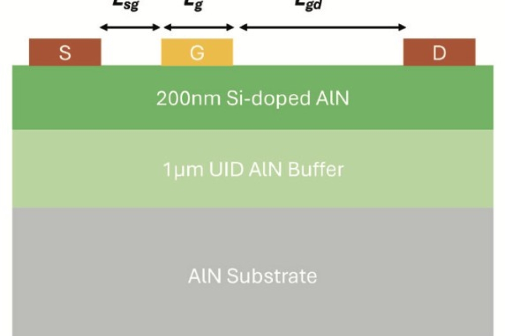
Breaking new ground, the team from Arizona State University has produced the first AlN-on-AlN MESFETs by loading 2-inch AlN substrates from Hexatech into an MOCVD reactor and depositing: a 1 µm-thick AlN buffer layer; a 200 nm-thick n-type channel layer with a silicon doping concentration of 1 x 1019 cm-3; and a 2 nm-thick GaN capping layer, added to protect the AlN layers from oxidation.
Characterisation of these epiwafers reveals a surface roughness, according to atomic force microscopy, of around 0.4 nm, and a dislocation density as low as 104 cm-2, based on X-ray diffraction. As this dislocation density is at least three orders of magnitude lower than that for AlN-on-sapphire structures, there is the promise of improved device performance.
Device fabrication began by cleaning the surface of the epiwafer, before turning to conventional photolithography and lift-off processes to form isolated mesas by etching to a depth of around 700 nm into the resistive buffer layer. Electron-beam deposition added all three contacts, with the source and drain formed first, with annealing under nitrogen at 950 °C for 30 s.
Electrical characterisation of the MESFETs revealed that the AlN ohmic contact is non-linear, a trait that is said to be typical for AlN and high aluminium content AlGaN, due to the high potential barrier at the metal-semiconductor interface. The team found that the resistivity of the contact falls at higher temperatures, thanks to an easier passage for the thermally excited electrons through the metal/AlN interface, attributed to tunnelling through an effectively thinner potential barrier and/or thermionic emission.
Measurements of output characteristics determined normally-on operation and effective modulation of the drain current by the gate-source voltage. Drain current peaks at 56 µA mm-1, a value six times higher than that reported for AlN-on-sapphire MESFETs. Fu and colleagues believe that this improvement stems from the lower sheet resistance in the homoepitaxial AlN layer.
Off-state breakdown of the team’s devices increases from 442 V to 2010 V as the drain-to-gate-spacing increases from 2 µm to 15 µm.
Fu says that his team’s transitors are still inferior to state-of-the-art SiC and GaN power devices, in terms of on-resistance and forward-current capabilities. “This is mainly caused by low electron carrier concentration and poor ohmic contacts in AlN devices.”
The team is now working on improving the doping efficiency and the ohmic contacts of its AlN MESFETs, to reduce on-resistance and increase on-state current. “And we are also developing AlN-based MOSFETs to realise more robust gate control,” added Fu.
Reference
B. Da et al. Appl. Phys. Express 17 104002 (2024)