Transforming the current density of AlN Schottky barrier diodes

Engineers from North Carolina State University and Adroit Materials have raised the bar for the current density of AlN Schottky barrier diodes by three orders of magnitude.
The team’s diodes, capable of operating at a current density of more than 5 kA cm-2, feature a highly doped Al0.75Ga0.25N contact layer and a lightly doped AlN drift layer. It’s a combination that can create an electron barrier at this interface – but is avoided by adding a compositionally graded layer, key to enabling a far higher forward current.
By delivering a dramatic increase in the current density of AlN Schottky barrier diodes, the team is helping these devices to fulfil their tremendous promise.
This class of diode has the potential to serve in high-voltage, direct-current power transmission and locomotive drive systems, where it could offer a breakdown voltage of more than 10 kV. Note that thanks to a breakdown field that’s greater than 16 MV cm-1 and a high electron mobility, AlN has a Baliga figure of merit more than 30 times that of GaN or SiC, enabling AlN devices with blocking voltages in the 10 kV range to have drift layers just a few microns thick.
Crucial to the fabrication of a high-performance device is an ohmic contact, realised with a quasi-vertical structure featuring a heavily-doped AlGaN layer as the contact layer.
To assess the impact of the AlN/AlGaN interface on the maximum forward current, the engineers carried out simulations using Silvaco TCAD software.
This modelling revealed that when there is an abrupt heterojunction, a sharp discontinuity is present in the band structure that introduces a barrier for electrons flowing from AlGaN to GaN. When operating under forward bias, this electron barrier is reverse biased and acts as a nonlinear series impedance. Inserting the compositionally graded layer eliminates the electron barrier.
Proof of the benefit of introducing the compositionally graded layer is provided by measurements on devices with and without this feature. Three different devices were fabricated: a control with a homoepitaxial AlN contact layer, another with an abrupt heterojunction, and a third with a graded layer heterojunction (see figure above).
All three variants were produced by loading Hexatech single-crystal AlN substrates with an average dislocation density of 103 cm-2 into an MOCVD chamber. After depositing an AlN-based stack on the substrate, the team processed the resulting epiwafers by photolithography and reactive-ion etching to form circular mesas, with electron-beam evaporation adding ohmic contacts.
Electrical measurements on these devices, which had radii ranging from 25 µm to 300 µm, revealed current scaling with the Schottky contact area for radii up to 50 µm. For radii larger than this, current density decreases with increasing device area.
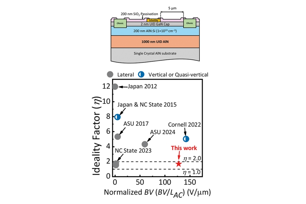
Plots of room-temperature current-voltage characteristics determined an ideality factor of no more than 1.2, and an on-off ratio in excess of 1011. This led the team to conclude that they had produced high-quality Ohmic contacts.
The team also found that the device with the graded-layer hetero-junction produced a current that’s a factor of 103 higher than that with the abrupt junction, and 104 higher than the control.
AlN-based Schottky diodes with the abrupt and graded hetero-junctions were also investigated with impedance spectroscopy. Plots uncovered a bias-dependent feature in the diode with the abrupt junction that’s attributed to the electron barrier. As this bias-dependent feature is not seen in the graded hetero-junction diode, the team concluded that this measurement offers further evidence for the hike in maximum current density stemming from either the reduction or removal of the electron barrier.
Despite the lack of edge termination to aid field management, the breakdown voltage of the diode is as high as 680 V, corresponding to a maximum electric field of 12.3 MV cm-1.
Reference
C. E. Quiñoes et al. Appl. Phys. Express 17 101002 (2024)


