SemiQ launches hi-rel 1700V SiC MOSFETs

SemiQ Inc, a developer of SiC devices has announced a family of 1700 V SiC MOSFETs designed to meet the needs of medium-voltage high power conversion applications, such as photovoltaic and wind inverters, energy storage, EV and road-side charging, uninterruptable power supplies, and induction heating/welding.
The high-speed QSiC 1700 V switching planar D-MOSFETs enable more compact system designs at large scale, with higher power densities and lower system costs, according to the company. They feature a reliable body diode, capable of operation at up to 175degC, with all components tested to beyond 1900 V, and UIL avalanche tested to 600 mJ.
The QSiC 1700 V devices are available in both a bare die form (GP2T030A170X), and as a 4-pin TO-247-4L-packaged discrete (GP2T030A170H) with drain, source, driver source and gate pins. Both are also available in an AEC-Q101 automotive qualified version (AS2T030A170X and AS2T030A170H).
The MOSFETs deliver low switching and conduction losses, low capacitance and feature a rugged gate oxide for long-term reliability, with 100 percent of components undergoing wafer-level burn in (WLBI) to screen out potentially weak oxide devices.
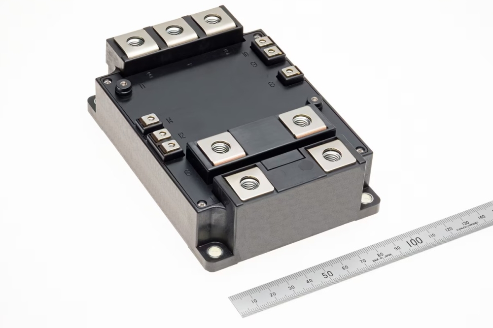
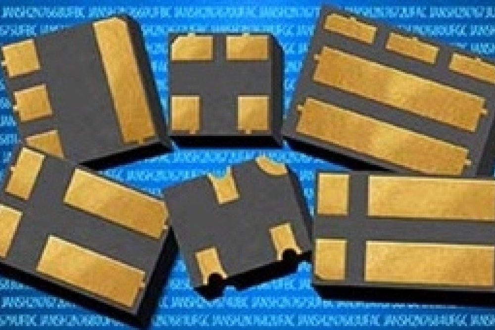
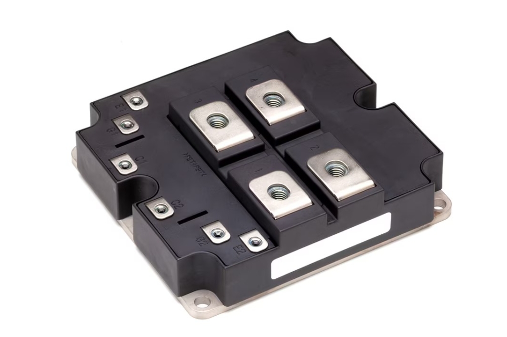
SemiQ has also announced a series of three modules as part of the family to simplify system design, this includes a standard-footprint 62 mm half-bridge module housed in an S3 package with an AIN insolated baseplate, as well as two SOT-227 packaged power modules.
The QSiC 1700 V series' bare die MOSFET comes with an aluminum (Al) top side and nickel/silver (Ni/Ag) bottom side. Both it and the TO-247-4L packaged device have a power dissipation of 564 W, with a continuous drain current of 83 A (at 25degC, 61A at 100degC) and a pulsed drain current of 250 A (at 25degC). They also feature a gate threshold voltage of 2.7 V (at 25oC, 2.1 V at 125degC), an RDSON of 31 mΩ (at 25degC, 57 mΩ at 125degC), a low (10n A) gate source leakage current and a fast reverse recovery time (tRR) of 17 ns. The TO-247-4L package has a junction to case thermal resistance of 0.27oC per watt.
The two 4-pin power modules are housed in a 38.0 x 24.8 x 11.7 mm SOT-227 design and deliver an increased power dissipation of 652 W with an increased continuous drain current of 123 A (at 25degC – GCMX015A170S1E1) and 88 A (at 25degC GCMX030A170S1-E1). In addition to low switching losses, both modules have a low junction-to-case thermal resistance of 0.19oC and 0.36degC per watt and feature an easy-mount design for direct mounting of the isolated package to a heatsink.
The half-bridge module is housed in a 61.4 x 106.4 x 30.9 mm 9-pin S3 package and delivers a power dissipation of 2113 W with a continuous drain current of 397 A and a pulsed drain current of 700 A. In addition to low switching losses, the GCMX005A170S3B1-N module has a junction to case thermal resistance of 0.06degC per watt.


