QPT solves heat removal in GaN electronics
As the power handled by transistors increases to meet the needs of new applications, packaging increasingly struggles to remove the waste heat from the die.
To address this, QPT has just filed a patent for a novel way to attach dies to the heat spreaders or substrates (typically Aluminium Nitride).
The technique, which it calls qAttach, conducts heat away from the die more efficiently and increases reliability because the assembly process places less stress on the substrates.
QPT developed qAttach process for use with the GaN transistors it uses in its electric motor control designs to enable them to handle the large amounts of waste heat from these high power, high voltage applications.
GaN transistors are now being made that are rated for high voltages but the die size is relatively small for high voltage transistors, which means there is less surface area to remove heat from. As a result, they are often down rated to enable them to function without overheating.
qAttach solves this problem opening up GaN to for use in for next generation, high power, high voltage applications in automotive, industrial motors and to finally deliver on the promise of low cost, high voltage GaN transistors, according to QPT.
Rob Gwynne, QPT’s CTO, said: “The problem with the current attachment approach is that the sinter layer, which fixes the die to the substrate, is typically 30 to 60 microns thick and this forms a thermal barrier that impedes the transfer of heat away from the chip. We use reliable, well-established technologies from other fields in a novel way to enable us to create the qAttach attachment layer that is potentially down to a fraction of a micron thick. This major reduction in the thermal barrier thickness means that our solution is up to ten times better at transferring waste heat away from the chip. As we refine the process, we are expecting even better thermal transmission rates through this layer.”
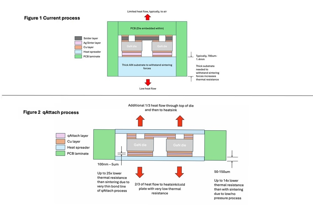
Gwynne explained that, with the conventional approach, the heat from the die has to pass through the thick sinter layer to the substrate to be dissipated via the heat sink as in figure 1 (above). The PCB is attached to the top (and around the heat spreader in embedded packages) so there is little heat dissipation that way.
QPT’s new structure in figure 2 (above) is a sandwich of heat sink, substrate, qAttach layer, die, qAttach layer, substrate and heat sink with the PCB surrounding the structure at the sides. Because the qAttach layer is ultrathin, heat can be transferred through and away much quicker plus this can also now happen from the top of the die to increase the total rate of heat removal by up to 15x.
This technology has other improvements over the current sintering process. Firstly, the substrate can be much thinner as the application of the large force needed by sintering is not required. The thinner substrate significantly reduces thermal resistance to further help heat transfer away to the heat sink.
Secondly, the lower pressure required for this process means that the manufacturing stresses on the dies are less. This reduces the possibility of device failure which will be of particular interest to automotive companies where reliability is key.
Thirdly, the ultrathin qAttach layer is not a laminar sheet. It has a proprietary geometry which constrains expansion predominantly in the Z axis, which is perpendicular to the qAttach layer, when heated, so delamination of the attach layer from the die and substrate does not occur which is a major issue with current attachment methods. This is because the conventional, continuous sheet of the sintered approach has about seven times the thermal expansion of the die and about three times that of the AlN substrate.
These differing rates of expansion create considerable stresses over the length of a large power die that can result in the structure ripping itself apart when heated. This delamination is the largest cause of failures in power packages so this new approach further improves the reliability of the assembled device.
Gwynne concluded, “Our new qAttach process is a universal solution to solving the growing problem of the removal of waste heat that would otherwise hold back the development of next generation, power electronics. The ability of qAttach to improve transfer heat away from the die by up to 15x can also be used to solve the removal of waste heat from almost any other type of transistors such as SiC to enable them to handle higher power loads than they can at present. We already have a couple of leading multinationals interested in licensing this process as they can see the strategic benefits that this innovation would bring to their product lines.”


