Na‑flux method improves GaN device performance
Toyoda Gosei has shown how a technology to enhance GaN substrates can improve device performance compared to commercially-available substrates in both power regulation capacity and yield ratio. The findings were published in Physica Status Solidi (RRL) – Rapid Research Letters.
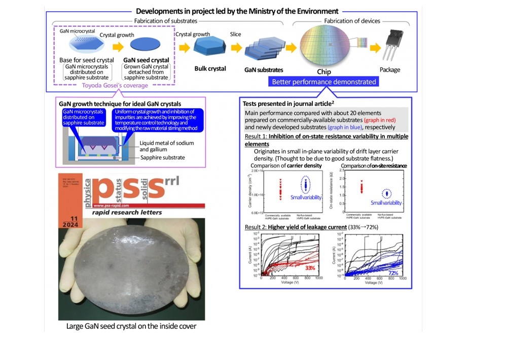
The result has come out of a Japanese Ministry of the Environment project looking at the wider application of GaN power devices, for which Toyoda Gosei is providing technology to obtain ideal GaN crystals using the Na‑flux method (a liquid phase epitaxy technique where sodium acts as the solvent to facilitate crystal formation).
Currently, 4 inch diameter GaN substrates fabricated by HVPE are commercially available, and it has been reported that 6 inch GaN crystals can be obtained using HVPE, while 7 inch GaN substrates can be obtained by tiling 2 inch GaN substrates. For thick film growth, thicknesses greater than 5mm have also been reported using the HVPE method.
The simultaneous growth of large quantities of GaN crystals achieved using the ammonothermal method can also reduce fabrication costs. Among these methods, the Na-flux method has attracted attention as a means of obtaining large-diameter, low-dislocation, and low-curvature GaN crystals.
Most reports related to the Na-flux method have dealt with the crystal quality; few have characterised GaN devices. This paper looks at both the structural quality of the latest GaN crystals grown using the method, and for the first time, the characteristics of a vertical transistor fabricated this way (see graphs above).
The vertical transistor produced on the Na-flux-based HVPE-GaN substrate exhibited normally off operation with a gate-voltage threshold of over 2 V and a maximum drain current of 3.3 A during the on-state operation, indicating the first vertical GaN transistor operation on a GaN substrate produced through the Na-flux method.
A breakdown voltage of over 600 V was confirmed based on the off-state characteristics, and a low leakage current was realised. The team also found that the on-resistance variation could be reduced by suppressing the effective carrier density variation using a GaN substrate with small off-angle variations.
In addition, the reverse I–V characteristics of the parasitic PN junction diode structures exhibited suppression of the number of devices with a large leakage current compared to the commercially available GaN substrate. According to the researchers, these results indicate the importance of low bowing and threading dislocation density (TDD) in GaN crystals.
Finally, the researchers demonstrated a circular GaN substrate with 161 mm diameter, surpassing 6 inches, grown by the Na-flux method, which is the largest GaN substrate except for those made through the tiling technique.
Reference
‘Characteristics of Vertical Transistors on a GaN Substrate Fabricated via Na-Flux Method and Enlargement of the Substrate Surpassing 6 Inches’ by Yusuke Mori, et al. 2024; physica status solidi (RRL) – Rapid Research Letters, Volume 18, Issue 11.


