Deepening the understanding of post-trench restoration
A detailed investigation offers new insights into the impact of wet etching during the fabrication of trench-based GaN-on-GaN power devices
GaN-on-GaN power devices, renowned for their high breakdown voltage, high current capability and excellent dynamic performance, often feature a trench architecture to improve performance. Typically defined by inductively couple plasma etching, this trench also increases leakage current while degrading channel and blocking characteristics, so wet etching with tetramethylammonium hydroxide (TMAH) is often employed to restore device performance. But what exactly happens during this anisotropic etching step?
Claiming to offer the most detailed answer yet to this crucial question is a team from Zhejiang University, China.
“Building on previous results, our work not only explores the relationship between corner morphology and electric field distribution, but delves deeper into the anisotropy of TMAH treatment, including differences in trench structure and surface morphology on a/m-plane sidewalls,” says team spokesperson Yanjun Li. She points out that previous studies have only focused on how TMAH treatment yields smoother trench bottom corners, thereby enhancing the device’s breakdown voltage.
The team produced trench structures through inductively couple plasma etching, using a mixture of chlorine gas and BCl3, and a SiO2 hard mask. Employing a chamber pressure of 10 mTorr, the team assessed the impact of etching at RF powers of 100 W and 20 W, inductively couple plasma powers of 150 W and 250 W, DC bias conditions of 300 V, 200 V and 95 V, and the use and absence of TMAH treatment.
A scanning electron microscope revealed the presence of micro-trenches in some samples, caused by deflected ions that bombard the bottom of the sidewall. These micro-trenches, which could lead to significant electric-field crowding in vertical GaN power devices, can be avoided with a low DC bias, realised by increasing the inductively coupled plasma power and decreasing the RF power.
Li and co-workers refined the profile of the trenches by wet-etching in a 25 percent concentration of TMAH at 85 °C for 1 hour. Inspecting these trenches with a scanning electron microscope showed that all sidewalls become more vertical after etching. However, the a-plane has sharp bottom corner, while the m-plane sidewall has a rounded bottom corner. According to Li, simulations and experimental results demonstrate that this anisotropy suppresses electric-field crowding along the m-plane sidewall, in contrast to the a-plane sidewall. “This highlights the need for paying attention to crystal orientation during the design and fabrication of vertical GaN power devices.”
The anisotropy introduced by TMAH treatment extends to sidewall surface morphology. This wet-retching step does not improve the striped, rough surface produced on the a-plane sidewall by the inductively coupled plasma, but TMAH treatment leads to a noticeably smoother m-plane sidewall.
“Typically, a smoother surface is beneficial for reducing scattering of carriers in the channel, thereby enhancing device conduction characteristics,” points out Li.
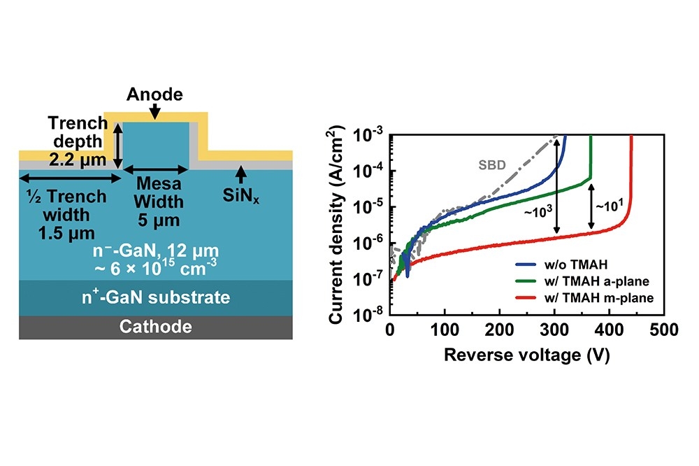
To assess the impact of post-trench treatment on reverse-blocking characteristics, Li and her co-workers produced trench MOS barrier Schottky rectifiers featuring a 12 µm-thick n-type GaN drift layer. For these devices, featuring a 2.2µm-deep trench with a mesa width of 5 µm and a trench width of 3 µm, electrical measurements highlight the benefit of TMAH treatment. This wet etching reduces leakage current, particularly along the m-plane (see Figure).
Additional work by the team involved the fabrication of metal-oxide semiconductor capacitors, used to determine the capacitance and the density of interface states of the mesa, trench bottom and sidewalls.
“The density of interface states for the etched sidewall is critical for vertical GaN power transistors, as the sidewall is typically utilized as the channel region,” says Li.
The team is now planning to employ its post-trench restoration process to the vertical GaN trench MOSFET, where the trench sidewall surface serves as the gate channel.
Pictured above: Wet etching quashes the reverse-bias leakage current in trench MOS barrier Schottky rectifiers.
Reference
Y. Li et al. Appl. Phys. Lett. 124 092103 (2024)