Hitachi Energy announces first 300mm IGBT wafer
Breakthrough will increase chip production capacity and deliver complex structures for 1200V devices
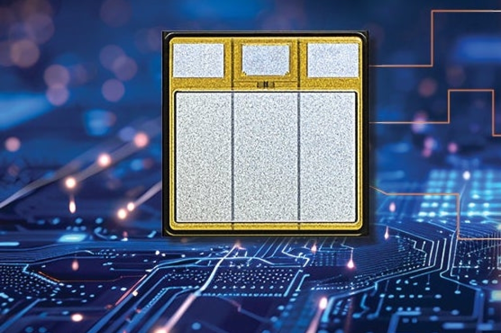
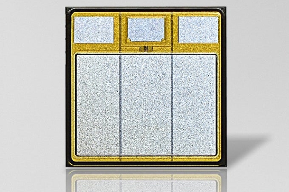
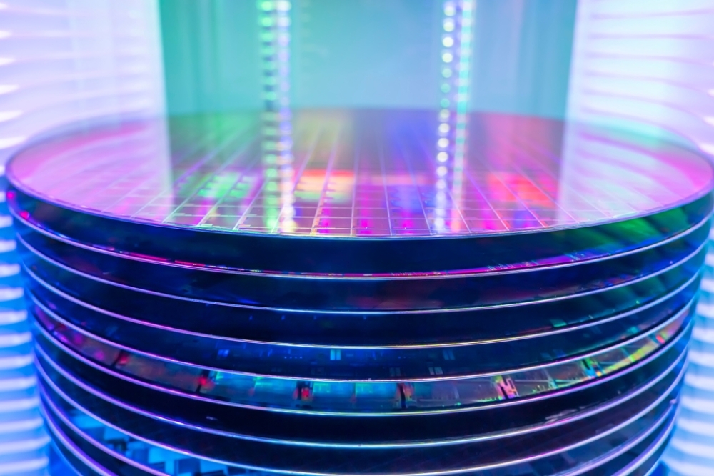
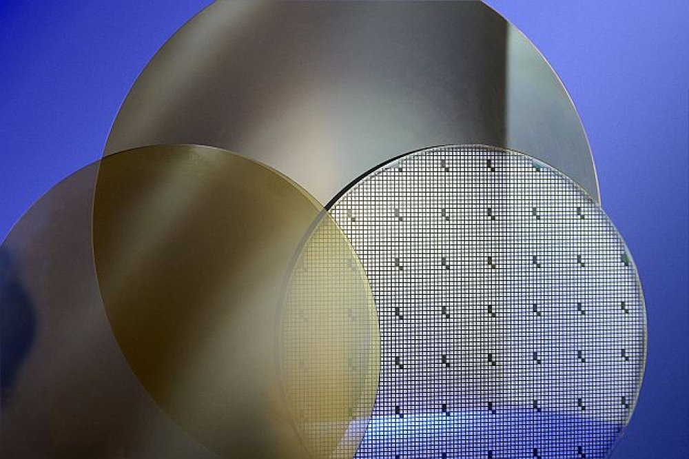
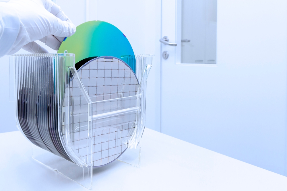
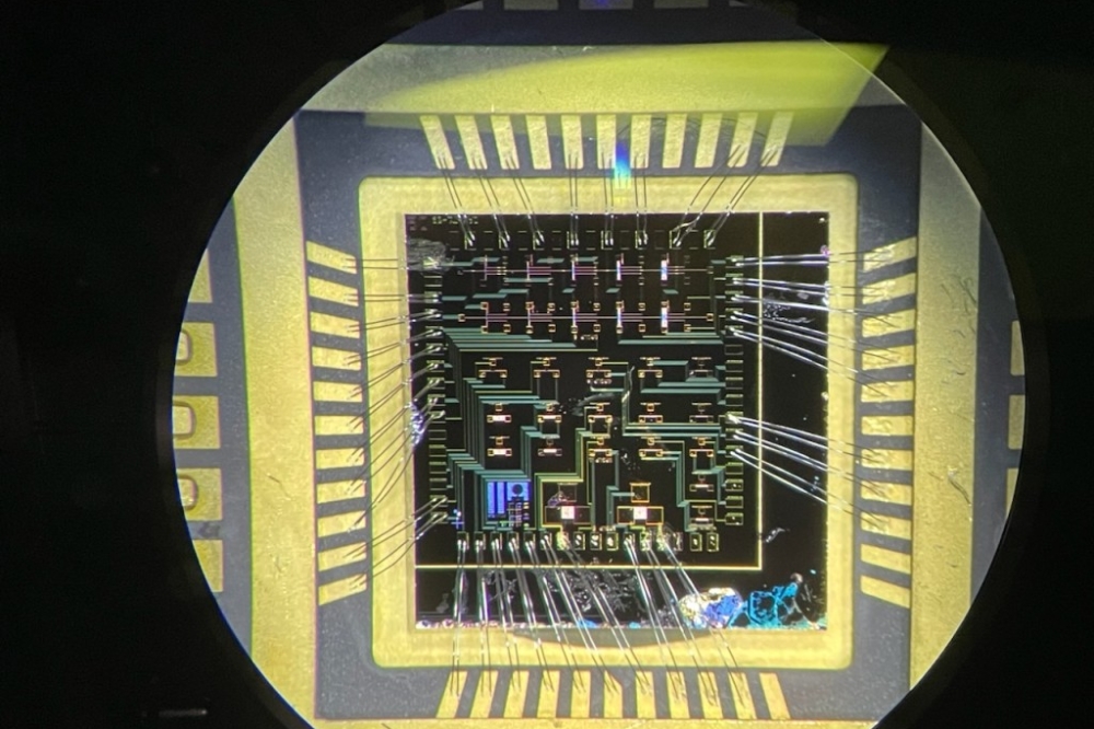
Hitachi Energy has achieved a breakthrough in its power semiconductor technology by introducing a 300 mm IGBT wafer.
The development will boost production capacity and enables more complex structures in 1200V IGBTs. Applications include variable frequency drives (VFD), uninterruptible power supply (UPS) systems, electric cars, trains and air conditioners, among others.
The larger wafer offers the potential to yield over double (2.4 times) the number of functioning integrated circuits per wafer as compared to the existing 200 mm wafer, leading to significant cost savings. It uses the latest fine pattern trench IGBT design, resulting in energy-efficient power conversion and control and minimising power losses during operations.
“It is impressive to see how seamless and fast the introduction of the 300mm wafers has been. The team’s success not only advances Hitachi Energy’s semiconductor technology but offers our customers enhanced competitiveness and capacity. In the future, we plan to expand our 300 mm wafer platform to support higher voltage IGBTs,” said Rainer Kaesmaier, managing director of Hitachi Energy’s semiconductors business.
Semiconductor experts at Hitachi Energy achieved the milestone through collaboration with a cross-functional team, including product management, business development, R&D, and a chip foundry partner.
Pictured above from left: Makan Chen, VP of sales & business development; Rainer Kaesmaier, managing director of semiconductors; Tobias Keller, VP of global Product management & marketing; Luca De Michielis, R&D team manager for BiMOS Chips, Roc Blumenthal, global program manager of Low Voltage IGBT


