AOS announces double-sided cooling DFN package

New top-exposed DFN 5 x 6 enables cooler, more reliable designs
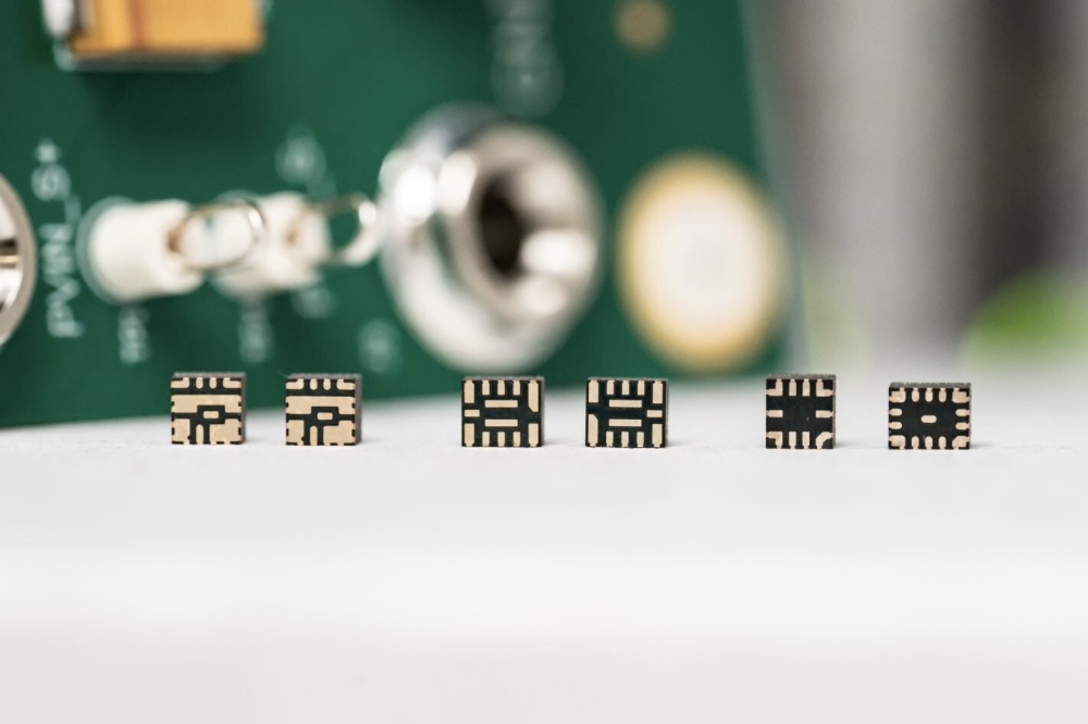
Alpha and Omega Semiconductor (AOS) has announced the AONA66916, a 100V MOSFET packaged in the company’s top and bottom side cooling DFN 5 x 6 package.
Typically, when using the standard DFN 5x6 package, the bottom contact is the main contributor for cooling, and most of the heat generated by the power MOSFETs will be transferred to the PCB. This increases the PCB thermal management design considerations to meet system requirements. AOS says its new top and bottom cooling DFN 5x6 package is designed to achieve the highest heat transfer between the exposed top contact and heat sink due to its large surface contact area construction.
This allows the device to achieve a low thermal resistance (Rthc-top max) of 0.5°C / W with results being transferred to the PCB board, enabling significant thermal performance improvements. The top exposed DFN 5x6 package of the AONA66916 shares the same 5mm x 6mm footprint as AOS’ standard DFN 5x6 package, eliminating the need to modify existing PCB layouts.
Another benefit of the AONA66916 is that it uses AOS’ 100V AlphaSGT technology, providing excellent FOM for balanced performance in hard switching applications. AONA66916 has a maximum RDS(on) rating of 3.4mOhms and has a 175°C junction temperature rating.
“Cooling the power MOSFET in high power design can be challenging, and AOS has successfully addressed this essential issue with our advanced top exposed package design. It not only enables better thermal transfer from its top side exposed contact to heat sink due to large exposed surface area, our new package delivers a much cooler device that contributes to a more efficient and robust final design,” said Peter H. Wilson, marketing sr. director of the MOSFET product line at AOS.


