Webinar: Sample preparation and TEM imaging techniques for advanced power devices
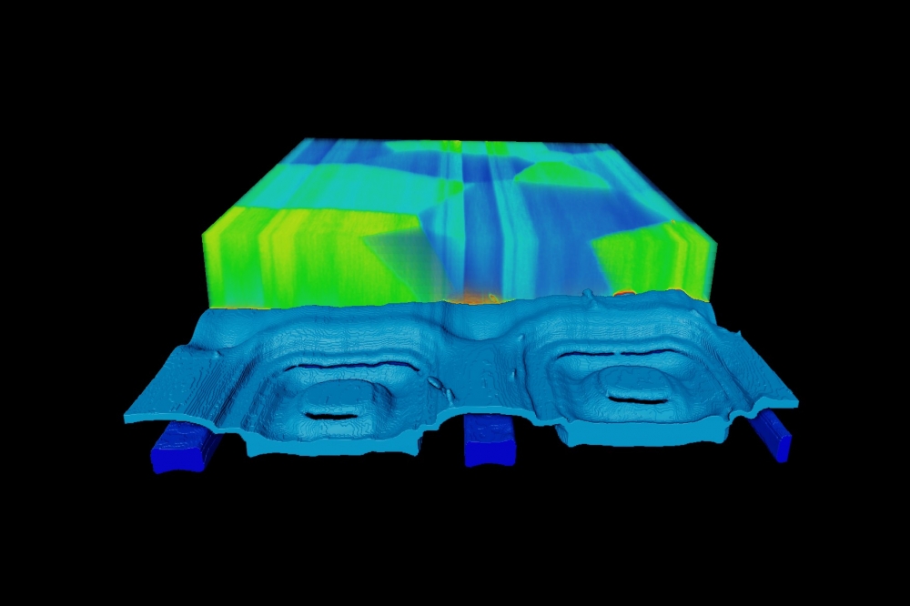
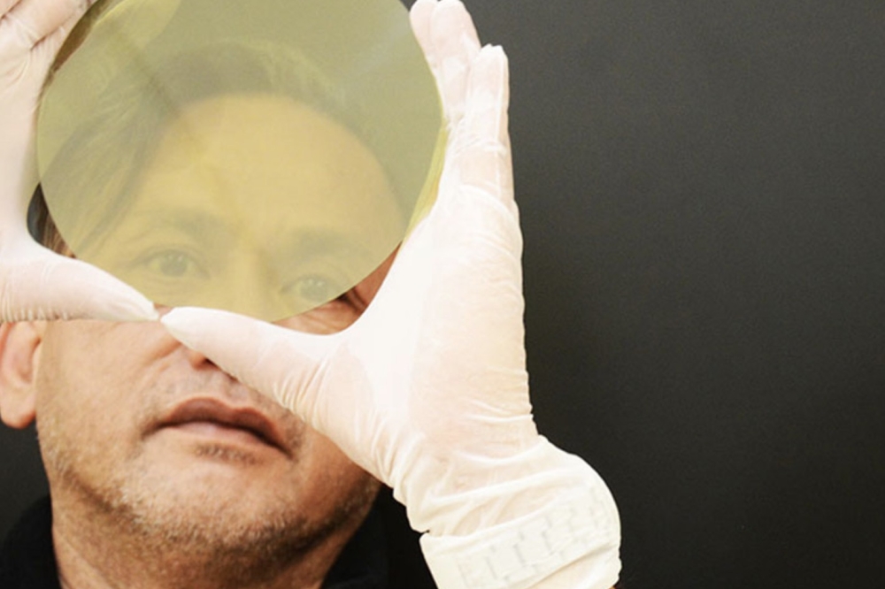
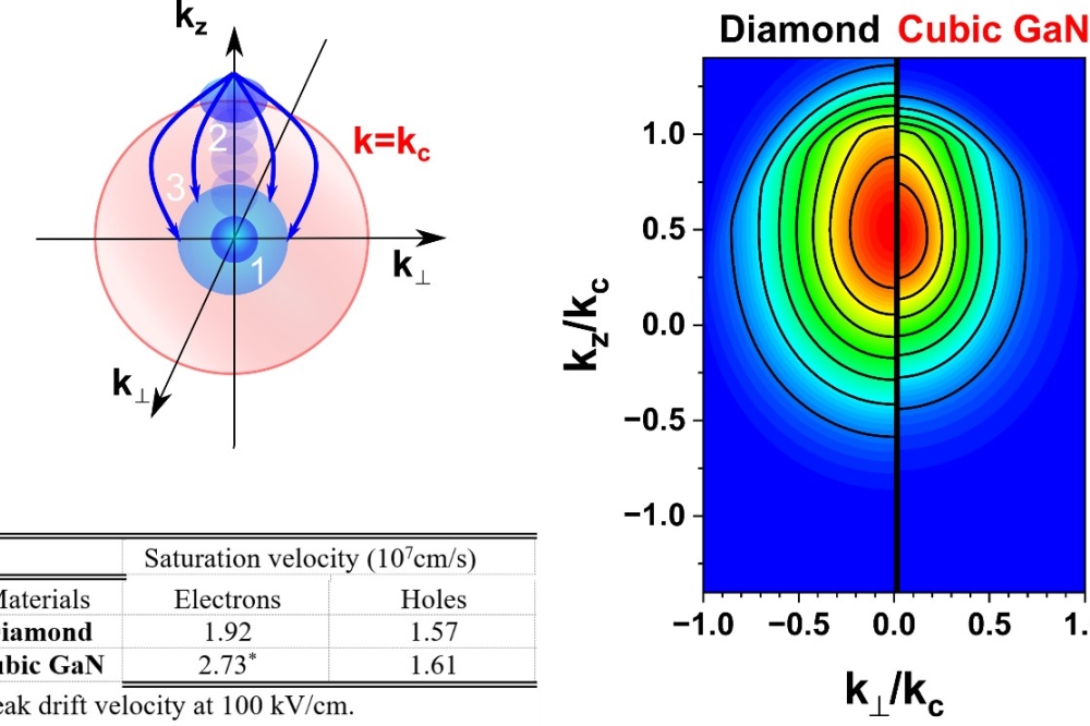
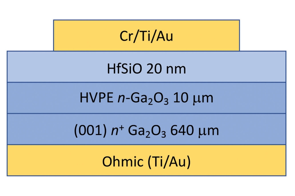
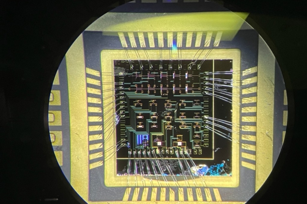
Compound semiconductors, like SiC and GaN, are increasingly attractive for their ability to operate at higher voltages, currents, and frequencies, especially in power and RF devices. However, fabricating wafers using these compounds has proven to be challenging, which can adversely impact manufacturing yield and costs. In addition to conventional semiconductor defects, one of the challenges is the presence of crystalline dislocations that are often difficult to identify and characterize.
This webinar will use real world use cases to discuss; defects including crystalline dislocations, cross-section and TEM lamella focused ion beam sample preparation, and the performance advantages provided by ion sources other than Ga+. We will also dive into the complexities and crucial requirements associated with (S)TEM analysis.
As you'll discover from this discussion, sample preparation and TEM elemental analysis serve not only as powerful tools for identifying and root causing defects but are essential for acquiring insights to inform and enhance manufacturing processes.
Who should attend this webinar:
• Power semiconductor manufacturers defect analysis and failure analysis engineers, managers, directors, failure analysis lab managers
• Substrate manufacturers failure analysis engineers, managers, directors, failure analysis lab managers
• Compound semiconductor researchers
By attending this webinar, you will learn about:
• Methods for identifying and root causing defects in power devices and substrates
• Techniques to improve cross-section and TEM lamella quality
• The performance advantages of alternative ion sources such as Argon and Xenon
• Key TEM analysis techniques for analyzing advanced power devices and materials
Free registration: https://angelbc.zoom.us/webinar/register/WN_JdrFfpLkSWGJYmjPl7GLaA#/registration