New 650V CoolMOS option targets fast EV charging
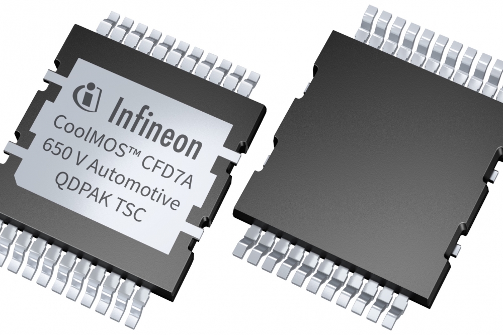
QDPAK package option offers improved electrical performance over TO247 THD devices
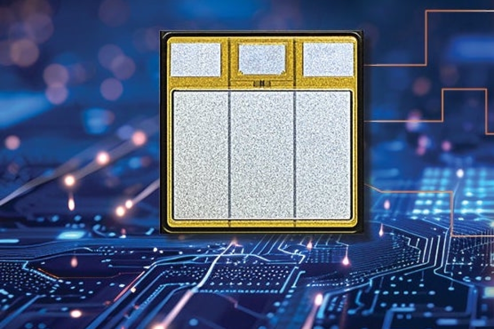
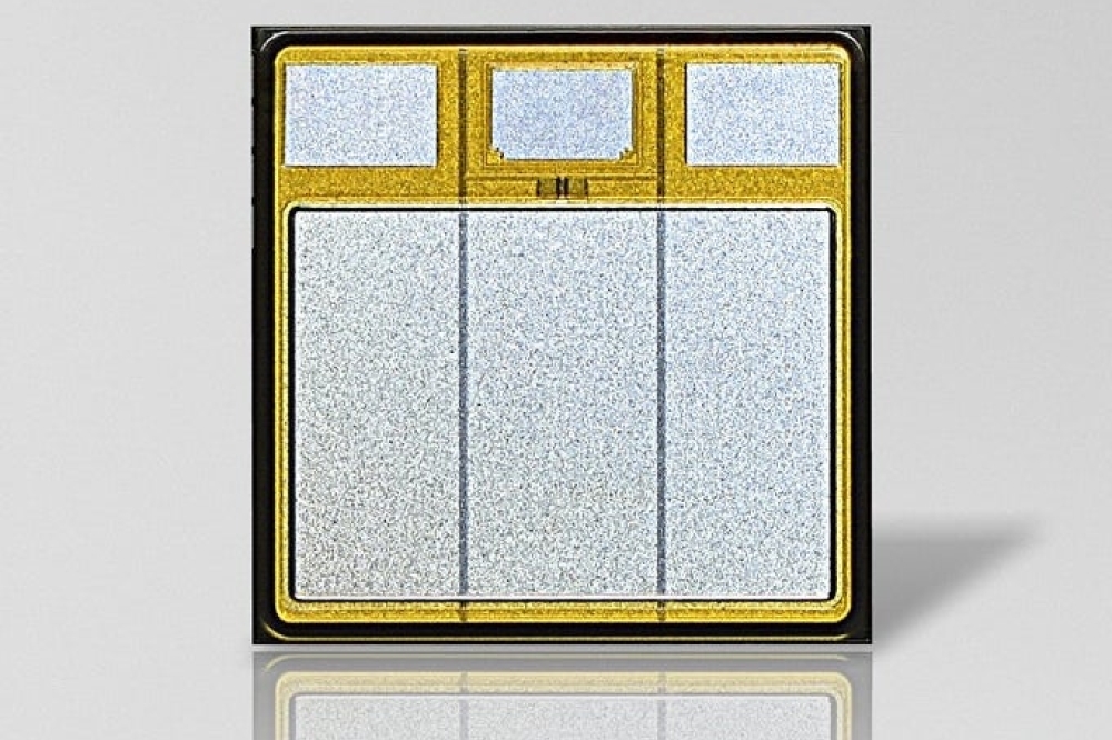
Infineon has expanded its 650V CoolMOS CFD7A portfolio by introducing the QDPAK package. This package family is designed to provide equivalent thermal capabilities with improved electrical performance over the well-known TO247 THD devices, enabling efficient energy use in onboard chargers and DC-DC converters.
The new addition complements the existing CoolMOS CFD7A series, offering versatility with top-side and bottom-side cooled packages. The QDPAK TSC (top side cooled), enables designers to achieve higher power densities and optimal PCB space utilisation.
According to Infineon, new system designs using 650V CoolMOS CFD7A in QDPAK TSC will maximise PCB space use, doubling power density and enhancing thermal management via substrate thermal decoupling. This approach simplifies assembly, eliminates board stacking and reduces the need for connectors, thereby lowering system costs. The power switch reduces thermal resistance by up to 35 percent, providing high power dissipation that outperforms standard cooling solutions.
This feature overcomes the thermal limitations of bottom side cooled SMD designs using FR4 PCBs, resulting in a significant boost in system performance. The optimised power loop design locates drivers near the power switch, improving reliability by reducing stray inductance and chip temperatures. Overall, these features contribute to a cost-effective, robust, and efficient system ideal for modern power needs.
The QDPAK TSC package has been registered as a JEDEC standard for high-power applications, helping to establish a broad adoption of TSC in new designs with one standard package design and footprint. To further to accelerate this transition, Infineon will also release additional Automotive Qualified devices in QDPAK TSC for onboard chargers and DC-DC converters in 2024, such as 750 V and 1200 V CoolSiC devices.


